 | 06 Jan 2026
Concepts for a cost-efficient, additively manufactured WR90 coaxial waveguide transition
Marius Falk
Simon Müller
Volker Lücken
Andreas R. Diewald
This publication focuses on the production of low-cost prototypes of coaxial-waveguide transitions (CWTs) that achieve the performance level of industrial WR90 and WR187 CWTs. The assembly consists of a specially designed coupling element in stripline technology that merges into an SMA connector. It is embedded into a 3D printed housing treated with a metallic surface finishing to achieve compatibility with hollow waveguides. In the first part of this study, a copper spray varnish is used to create a conductive surface on the device under test (DUT). After assembly of the prototypes, network parameters will be extracted for one pair of transitions by carrying out a set of 2-port measurements. The individual performance of a singular DUT is then deembedded by using reference measurements of commercial-grade waveguides. This analysis shows that also S-parameter extraction on connectors with a poor transition is valid. Subsequently, the procedure for the developed WR90 CWT is applied to a WR187 waveguide standard, again followed by a performance analysis. The procedure briefly addresses the modified parameters and illustrates the results as S-parameters. A comparative analysis of the measurement results for each deembedded WR90 and WR187 prototype respectively, indicates a better performance for larger waveguide standards. In consistency with this observation, larger relative tolerances in manufacturing and difficulties in controlling a uniform metallization process are identified as the limiting factors of miniaturization. In the second part of this work, an alternative concept utilizing aluminum coating and a segmented manufacturing approach is developed, targeting reduced insertion loss but keeping the mechanical tolerance level. The redesign is based on the geometry of the prior WR90 prototype, but forming a plug-in kit with each body segment being clad in multiple thin layers of aluminum foil. The measurement results of these samples reveal the effects of increased conductivity and reduced irregularities in terms of significantly improved reflection and transmission parameters. The DUTs investigated in the third part of this work again originate from the initially manufactured variants. To investigate the effects of different metallic coatings, the copper varnish is now replaced by a silver based ink, which provides high conductivity and is therefore commonly used in additive manufacturing. The network measurements are repeatedly carried out with a varying number of layers of lacquer applications on the body's surface. By deembedding a singular part from the measurements, it is shown that increasing surface conductivity leads to a significant impact on transmission parameters. In direct comparison, the silver coated CWT outperforms both preceding variants with copper varnish or aluminum clad. With more than 95 % transmitted power, it is indeed competitive compared to the industrially manufactured WR90 CWT reference. To conclude, the study focuses on a comparison of three different additive manufacturing processes for equal hollow waveguide geometries at moderate frequencies. It proves that CWT parts are producible in a simple and rapid process. The production stages with the strongest impact on performance are identified and demonstrated to be controllable. The variant presented finally is able to achieve competitive performance compared to commercial-grade parts, especially when considering the enormous cost reduction. In addition, it is proven that the RF parameter extraction method for symmetric two-port networks presented earlier by the authors is also applicable when the DUT exhibits high insertion losses.
The central aim of this work is to demonstrate that additive manufacturing combined with low-cost metallization techniques can produce coaxial-waveguide transitions that approach the performance of industrial WR90 standards.
This novelty highlights the feasibility of achieving near-commercial-grade quality at a fraction of the cost, thereby extending the accessibility of high-frequency components to research and prototyping applications.
- Article
(2454 KB) - Full-text XML
- BibTeX
- EndNote


Coaxial-waveguide transitions (CWT) are complex yet crucial connections between two different waveguides. They are widely used in telecommunications, radar systems and various levels of microwave technology demanding high precision. The primary requirements for achieving high-quality connections are reflection- and loss-minimized transmission. In the production of commercial waveguide components, precise manufacturing techniques are utilized to ensure accurate dimensions. These techniques include various methods such as machining, casting or welding, depending on the specific requirements of the component. By employing these techniques, small dimensions can be maintained with high precision. A newer alternative associated with the progress of additive manufacturing is the production using 3D printers. This method allows for the immediate fabrication of casings and components using metallic materials or conductive filaments. Additionally, it provides the producer with the ability to directly influence the product. For instance, waveguide pieces as in Santiago et al. (2023) and related components like antennas (Goode and Saavedra, 2022) can already be printed. Apart from adhering to specific dimensions, it is also crucial to ensure a low reflection transition of the incoming power. This requires impedance matching between the coaxial cable and the waveguide, which is achieved by carefully designing and fabricating the components to have compatible impedance values. In literature, transitions can be reached through optimized termination of the inner conductor of the coaxial line (Enayati and Zarifi, 2022), adjustments made by inserting a microstrip line with an attached step transformer (Montejo-Garai et al., 2020) or directly through transformer structures fabricated using planar circuit technology (Pérez-Escudero, 2018). In addition to reflection, also transmission, dependent on the materials used and their properties, plays a vital role in power transfer within waveguide systems.
In this publication, the question is examined whether the production of a low-cost CWT of equal quality compared to industrially manufactured ones is possible using low-cost methods. The prototypes presented below have been designed using simplest manufacturing processes, inexpensive materials and a straightforwardly designed impedance matching element on a low-cost PCB process which has been used for all variants.
At the beginning, the characteristics of industrial CWT are determined using the approach to calculate RF parameters of a DUT from a set of 2-port network measurements as presented in Müller and Diewald (2015). Following this, after modeling, simulation, and construction, the performance of these cost-efficient prototypes is analyzed and evaluated using the same deembedding method.
Section 2 starts with an examination of the modeling and development of WR90 CWT prototypes in simulation. The manufacturing is explained in Sect. 3. Thereafter, an investigation into the extracted S-parameters of the fabricated prototypes is conducted in Sect. 4. Subsequently, the investigation for the loss process is done by adapting the original WR90 model to larger waveguide standards using WR187 CWT as an example in Sect. 5. The results are recalculated and discussed according to the deembedding method applied in the WR90 prototypes. In the following, two alternative assembly and metallization methods for the WR90 prototypes initially considered will be revisited in Sects. 6 and 7. Finally, there will be comparisons of the performances again and final assessment of the prototypes based on performance and application, as well as advice for further perfecting and thus approaching industrial standards.
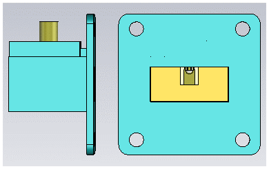
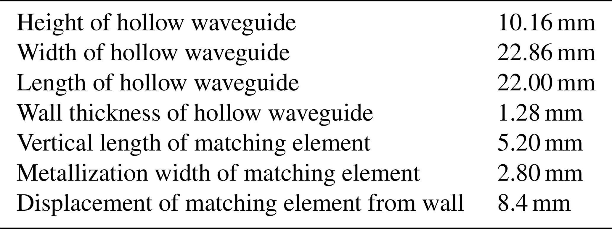
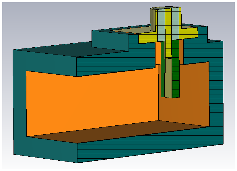
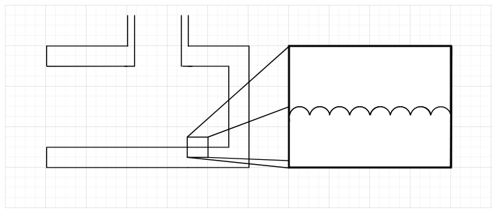
In the beginning, a model of the prototype is designed in CST Studio Suite 2022 (CST). As a reference, a WR90 waveguide and a SMA connector are given. For the waveguide, polycarbonate is chosen as the housing material and copper is chosen as conductive layer. For the coaxial port, a SMA-connector (SC7505 Data Sheet, 2024) from the supplier Fairview Microwave is chosen. The designated connector is reconstructed as a perfect electric conductor (PEC) according to the required dimensions and properties based on the available datasheet and 3D model. To reliably fix the coaxial cable to the hollow waveguide, a mechanical embedding is proposed in which the coaxial cable is inserted and secured with a plastic cover. A first simulation is carried out using a frequency domain solver, which logically provides poor values for the S-parameters due to the lack of adjustment. The construction of the completed simulation model can be seen in Fig. 1. The metallized plastic housing is indicated by cyan color and is first modeled with PEC to suppress losses and to show the general functionality. In order to achieve a suitable transformation of the impedance of the coaxial cable to that of the waveguide, a PCB-based matching element shall be used which can be seen (rectangular element with brown and white color) in the middle of the waveguide transition on the right side of Fig. (1). In conventional waveguide-to-coaxial transitions, these are components attached to the inner conductor of the coaxial cable in the form of steps (Simone et al., 2021) or protruding probes as performed in Bialkowski (1995). Since the manufacturing process aims to reduce overall costs, a matching element in the form of a planar transmission line is designed. The size and dimensions of the circuit board are optimized in CST using parameter sweep and manual optimization.
The design resembles that of a patch antenna from the front and only differs in the type of ground plane used. Instead of being continuously distributed over the substrate, the ground plane occupies only a small area opposite the patch and acts as a reflector. The results show, as expected, satisfactory values for the S-parameters. Subsequently the possible impact of 3D printing and sprayed metallization could be simulated by changing the material properties of the conductive layer in the simulation but the relevant material parameters are unspecified in the data sheet of the copper spray varnish. Thus the simulation is adapted to 10 % of copper conductance in order to include losses. The dimensions of the simulated and the 3D printed plastic components are given in the following Table 1.
After optimizing the coupling element and simulating some potential issues, the manufacturing of the waveguide housing continues with 3D printing.
3.1 3D-Print
Preparation of 3D printer commands is done by exporting the waveguide body used in the simulation into the slicer software UltiMaker Cura 5.4.0, utilizing STL mesh data as file exchange format. The orientation of the object is adjusted in a way that no support structures need to be printed within the field area to avoid unnecessary disturbances and irregularities. In addition, the contact surface of the upward-facing flange can be more evenly finished by using the “smoothing” function. Subsequently the printing process is carried out using a PLA filament and the Creality Ender-3 V2 3D printer. Due to initially significant deviations between the model and the print, the model dimensions need to be adjusted again and reprinted. Anyway, this adjustment does not guarantee 100 % accuracy, but the deviations could be narrowed down to a range of ±100 µm which is given in the data sheet of the printer. Alternatively, the settings of the 3D printer can also be adjusted. Finally, any fine irregularities and protrusions are carefully corrected using a mechanical file.
3.2 Metallization
After the printing process, a conductive coating of copper is applied to the waveguide body. For this purpose the conductive copper spray paint EMI 35 (EMI35 Data Sheet, 2024) from the company Kontakt Chemie is used. This is done by spraying multiple layers, ensuring that the layers are applied evenly to achieve uniform conductivity.
3.3 Assembly
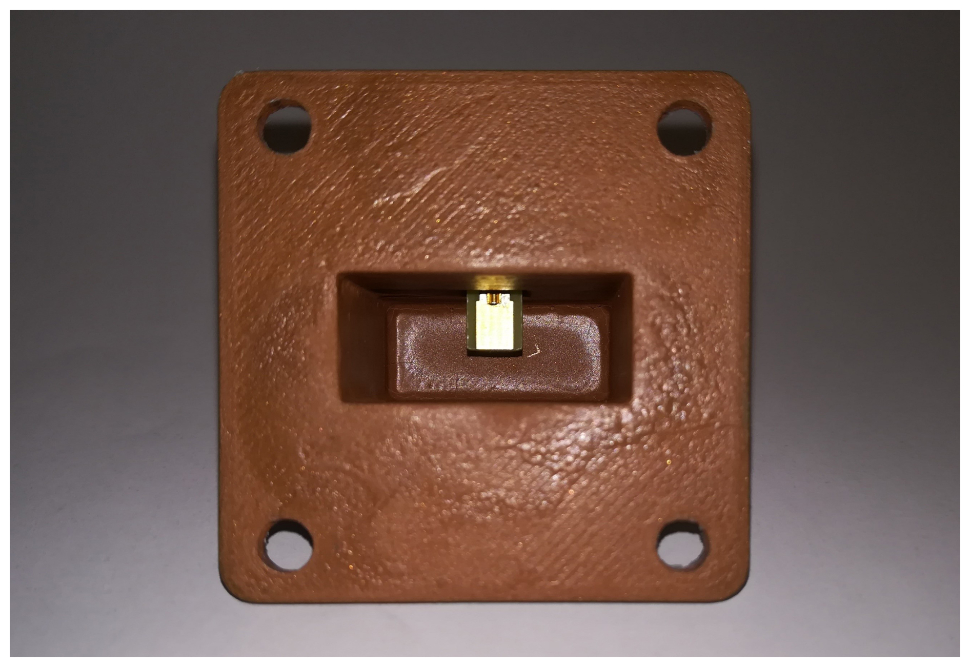
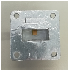
The previously developed coupling element in stripline technology is designed in KiCad and manufactured by Eurocircuits GmbH in Germany. Impurities and unevenness are again manually corrected using a hand file. By applying a fine hand file, the surface roughness can be reduced well below the initial 100 µm level (approx. down to 10–20 µm), although this manual post-processing only improves local surface quality and does not compensate for dimensional offsets or manufacturing tolerances. The strip line is then soldered to the coaxial conductor according to the simulation. At the end, the SMA connector is inserted into the designated opening of the printed waveguide along with the soldered strip line and it is secured in place using the printed sliding cover. Figure 2 displays a finalized prototype.
In order to compare the performance of the prototypes with that of a professionally manufactured CWT, the S-parameters of a commercial WR90 CWT (FMWCA1107 Data Sheet, 2024) from the provider Fairview Microwave is also recorded. The Vector Network Analyzer (VNA) ZNB40 used for the measurements by Rohde & Schwarz is allowed to warm up sufficiently and calibrated using the Through-Open-Short-Match (TOSM) method. The measurement setup always involves measuring two identical prototypes or commercial CWTs in a frequency range of 5.3 to 15.3 GHz. Since the commercial CWT is manufactured using automated processes and high-quality materials, it can be assumed that it possess sufficient accuracy in terms of symmetry and construction. Therefore, it is possible to accurately determine the S-parameters of an individual commercial CWT, as shown for S11 and S22 in Figs. 3 and 4, by applying the approach to calculate RF parameters of a DUT from a set of 2-port network measurements as presented in Müller and Diewald (2015). The methodology can be used for transmission line systems despite the limited applicable transmission theory, as the scattering parameters provide a connection between the incoming and outgoing powers, which are also clearly definable for waveguide systems.
In the following, the methods to determine the properties of the low-cost prototypes are given. On the one hand, the extraction of S-parameters are based on a measurement of a symmetrical setup with two similar prototypes. This method is called the “Extraction Method”. On the other hand, one single prototype is measured with a commercial CWT and afterwards the known S-parameters of the commercial CWT are deembedded, so we call it “Deembedding Method”.
4.1 Extraction Method
The assumptions made for the extraction are the geometric matching and reciprocity of the connectors measured together (M1), here CWT, as well as the use of a matching transmission line (M2), here waveguide disc. By the measurements M1 and M2, the systems of equations formulated considering the assumptions mentioned before can be solved using either the T-Parameter-Method or the Even-Odd-Method, which are described in detail in Müller and Diewald (2015). The chosen method is of secondary importance as the results must be identical. The S-parameters of the commercial CWT and the individual prototypes extracted in Figs. 3 and 4 are calculated using the Even-Odd method.
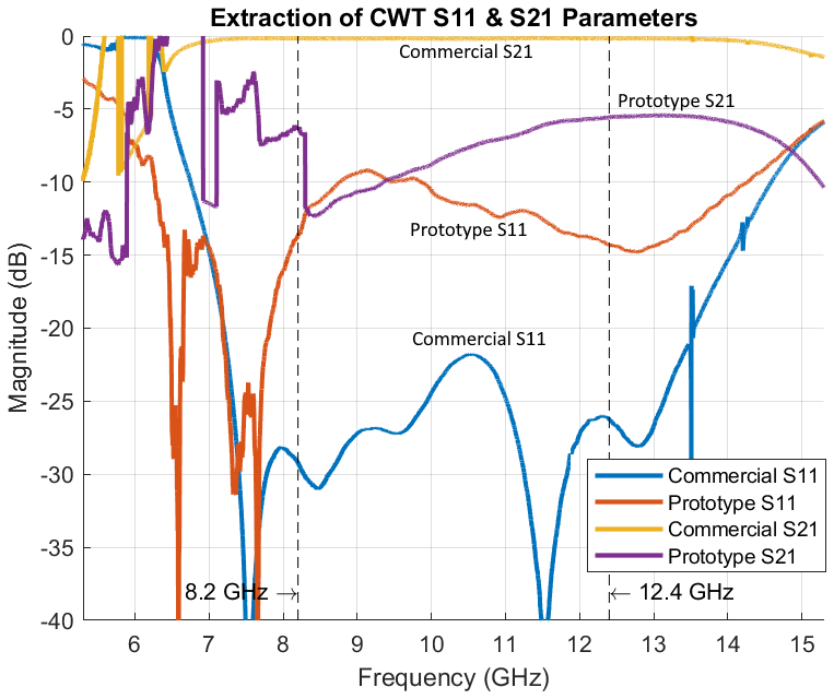
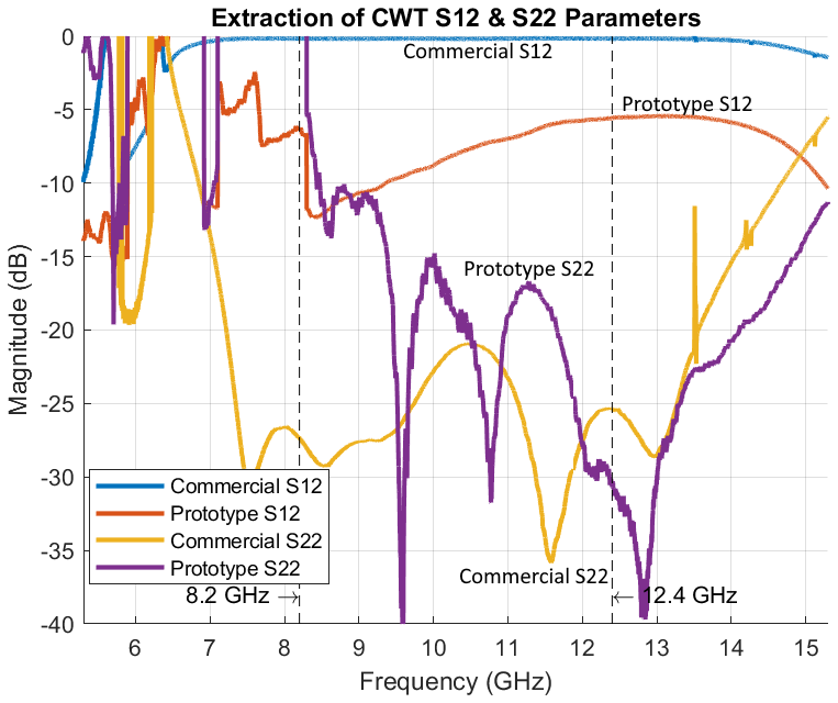
Considering all S-parameters at the beginning of the first third of the frequency spectrum, it is obvious that the extraction method does not work adequately below the cutoff. The reflection and transmission parameters of the extracted commercial CWT meet the VSWR of 1.25:1 and the maximum insertion loss of 0.2 specified by the manufacturer in the X-frequency band. For the prototype, the reflection parameters should be considered individually, as the values greatly differ. While the S11 parameter in the entire X-band only ranges from −9 to −14 dB, the S22 parameter predominantly falls below the −15 dB mark. The transmission parameters are, as this is an intrinsic property of a reciprocal (i.e. commonly passive) network, identical to each other according to the extraction method performed in the same way, and they range from −12.5 to −5.5 dB in the X-band. Before a conclusion is drawn about the prototype, it is necessary to revisit one of the fundamental prerequisites of the methodology, symmetry of the test setup. The solution to the equation systems is based on the fact that the combined measured CWT are exactly identical and therefore assign the same S-parameters.
This applies to commercial CWT under the assumption of machine manufacturing techniques and the use of high-quality materials, but not to the prototypes. To obtain unambiguous results for the S-parameters of prototypes, they must be deembedded once again.
4.2 Deembedding Method
Based on a high precision of the extracted S-parameters of the commercial CWT, another measurement (M3) between the commercial CWT and the manufactured prototype can clearly determine the S-parameters of the supposedly identical prototypes.
Equation (1) presents the scattering transfer parameters (T-matrix) of the overall S-parameter measurement of the commercial CWT mounted onto the manufactured prototype. Those parameters represents the concatenation of the individual transfer parameters of the commercial CWT and the manufactured prototype by a classical matrix multiplication of transfer parameters (Pozar, 2020). For this, the S-parameters of each two-port must be transferred in transfer parameters before. Equation (1) which corresponds to measurement M3 must be rearranged according to the T-matrix of the prototype. The determined T-matrix is rearranged once more before being converted into the S-parameters according to Müller and Diewald (2015) under the assumption of reciprocity for geometrically similar and symmetrical connectors. The S-parameters comparison of the extraction method and the deembedding method for the manufactured prototype is shown in the following Figs. 5 and 6.
Figure 5 shows the S11 reflection and the S21 transmission parameter for the manufactured prototype three times. The dark blue line indicates the S11 reflection based on the extraction method. With this method only one single function of S11 over frequency is calculated due to the assumption of symmetry by concatenation of two nearly identical protoypes I and II. The red line represents the S11 reflection of prototype I measured with the commercial CWT while the orange line represents the S11 reflection of prototype II measured with the commercial CWT, both calculated via the deembedding method. In the same Fig. 5, the S21 transmission parameter is given with the purple line indicating the transmission based on the extraction method of the symmetrical structure and the light blue and green line representing the transmission parameters based on the deembedding method of prototype I and II respectively.
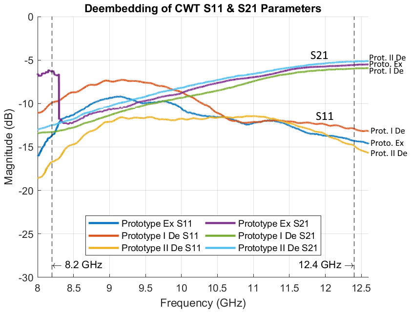
At first glance, the assumption that the individual S-parameters of the prototypes should not be considered identical is confirmed. Furthermore it is noticeable that the results of the extraction methods are between the results of the both prototypes found by the deembedding method.
Thus it is obvious that production tolerances of the prototypes yields a strong variation in reflection, especially below 10.5 GHz. Also for the transmission a variation of 1.4 dB is found. Nevertheless, the result of the extraction method seems to be an average of the results of the deembedding method as an symmetrical setup is assumed but which is not true due to the variation.
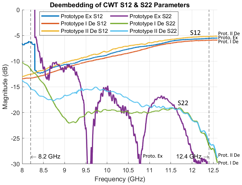
Figure 6 shows a comparable situation concerning the transmission parameter S12 for both methods. Regarding the reflection parameter S22 the extraction method fails, because the “inner” reflection could only be measured through the connector/transition itself. While the commercial CWT is able to bring enough power towards the inner port 2 of the prototype, the prototype itself is not feasible to do so.
Thus, the deembedding method is advantageous compared to the extraction method but which requires a commercial CWT to measure the prototypes while the extraction methods allows measuring the prototype without any commercial transition itself.
The performance evaluation of the S-parameters is done using the following Table 2.
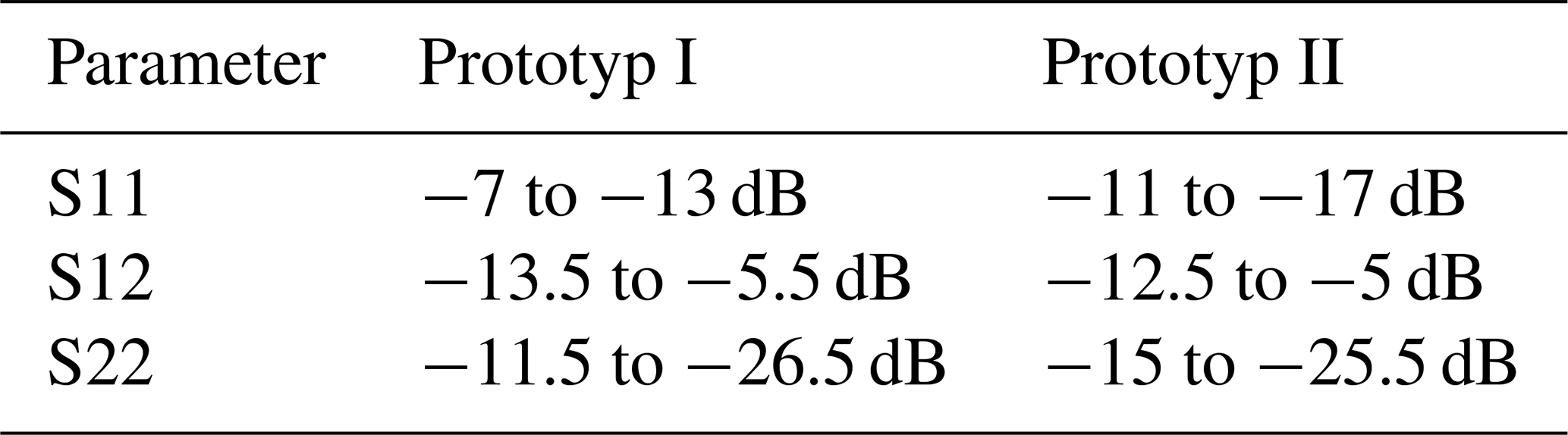
Based on the S-parameters, the corresponding reflected and transmitted powers can be assigned and evaluated to the prototypes. The prototype II reflects 2 %–7 % of the incident power at the coaxial port (S11) and only 0.3 %–3 % at the rectangular waveguide port (S22). The former values are within a moderate range while the latter can be considered very good. Less optimal is the performance within the prototypes. Only 5.6 % to 32 % of incident energy is present at the opposite port. These values are not sufficient and do not allow for any application. Considering the inadequate performance of the prototypes the construction and metallization need to be declared as a significant impact.
The next step involves transferring the scheme of previously developed low-cost WR90 prototypes to other waveguide standards, using the example of the WR187 standard. The starting point for the development of adapted prototypes for other frequency bands is a predecessor model of the WR90 CWT designed in CST. It consists of the housing made of 30 µm thick copper, covered by the shell of polycarbonate, the SMA connector with a line resistance of 50Ω, a protruding inner conductor and a rectangular contact surface. It also includes the previous self-developed coupling element in strip conductor technology. The described model shows Fig. 7 in cross-section.
It is deliberately chosen to use a simplified previous model, as subsequent modeling of details such as solder masks or solder, anyway requires individual adjustments for each prototype according to different waveguide standards.
5.1 Variation of the WR90 prototype
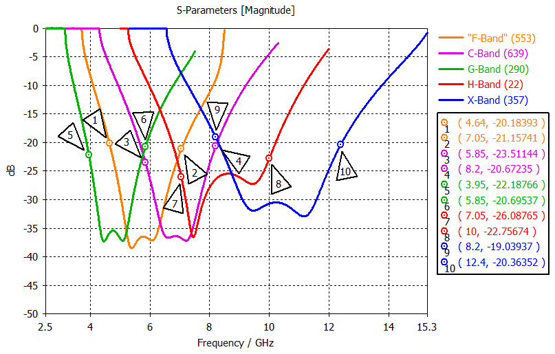
Upon transitioning from the X-Band of the WR90 waveguide to the G-Band of the WR187 waveguide, three more frequency bands - H-Band, C-Band, and F-Band – are traversed, as specified by the manufacturer of Millimeter Wave Products (Waveguide Data Sheet, 2024). The process of transferring waveguide standards into each other is done by changing the dimensions of the waveguide part proportionally to the wavelength, followed by the similar adaptation of the coupling elements in strip line technology. The measures to ensure impedance matching in the new frequency ranges are based only on variations in length, position and impedance transformation of the coupling element, similar to those in Dewantari et al. (2019) as a variation in PCB substrate thickness is not possible. The performance of the coupling element is again optimized by a parametric study in CST MWS. The simulation results for different waveguide standards is shown by the S11 parameters exemplified in Fig. 8.
The final adjusted simulation results of the WR187 prototype will be listed during the later deembedding of the performances. The construction of two WR187 prototypes following the modeling and simulation is carried out using the method from the previous finished WR90 prototypes with 3D printing, copper spray and fixation of the SMA coupling element.
5.2 Results
After completion of production, the new WR187 prototypes (two samples I/II), along with a commercial WR187 CWT (FMWCA1076 Data Sheet, 2024), are measured using the ZNB 40 Vector Network Analyzer (VNA).
The performance of the manufactured prototypes can then be deembedded from the measurement results by applying the extraction method according to Müller and Diewald (2015) to the commercial WR187 CWT again. An overview of achieved performance for the new WR187 prototypes compared to simulation and the discussed WR90 prototypes are shown in Figs. 9 and 10 based on the S11 and S21 parameters.
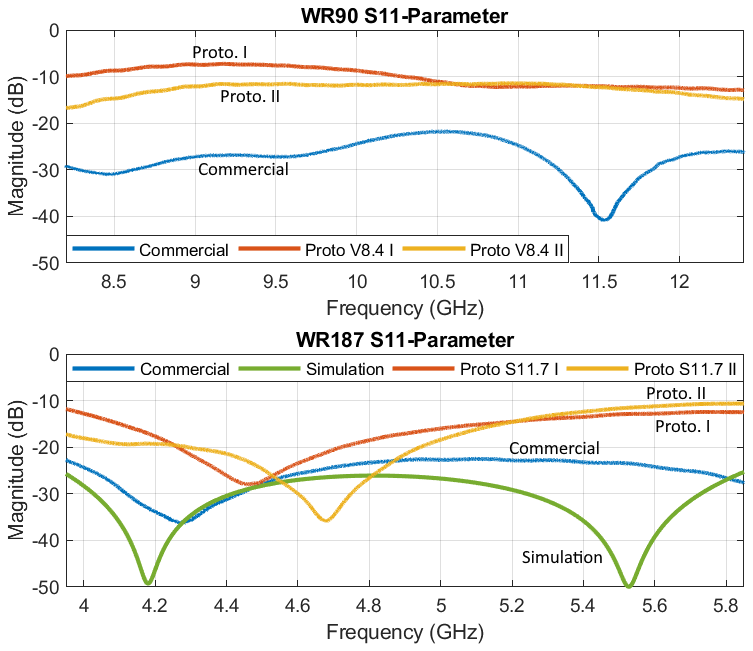
Figure 9Comparison of S11 Parameter for WR90 (all measured by dembedding method) and WR187 Prototypes (measured and simulated).
The S11 parameters of the WR187 prototypes are shown for the simulation and the measurement results found by the deembedding method in the lower part of Fig. 9 together with the S11 parameter of the commercial CWT. The measured result consistently fall below the −10 dB threshold, unlike the WR90 prototypes for which the measured reflection parameters are found in the upper part of Fig. 9. However, they still exhibit significant discrepancies compared to the simulation and quality of the commercial CWT.
The comparison of the S21 parameters shown in Fig. 10 indicates an comparable behaviour for the transmission of the prototypes. The WR187 standard has a higher transmission factor (from −7 up to −3 dB) compared to the WR90 standard (from −13.5 to −5 dB). Both prototypes are not reaching the performance of the commercial CWT which is given around 0 dB for both standards.
Consequently, the performance of both standards is generally too lossy to be professionally applicable, except in areas where the reflection attenuation exceeds 20 dB (approximately 4.3–4.9 GHz). The unsatisfactory results can be attributed once again to the low-cost production mainly based on manual manufacturing as discussed before. The deviations of the real material properties from those assumed in the simulation play a significant role too. It is particularly noteworthy that the metallization of the copper spray, in particular the conductivity, is once again insufficient.
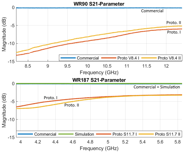
Figure 10Comparison of S21 Parameter for WR90 (all measured by dembedding method) and WR187 Prototypes (measured and simulated).
The transmission parameters as seen in Fig. 10 do indeed improve from WR90 to WR187, but this is due to the larger dimensions and lower frequencies of the WR187 standard. The general increase in transmission parameters with frequency can be explained by the decrease of waveguide dispersion. The waves tend to propagate more linearly through the waveguide and reflect less at the copper walls.
5.3 Comparison of Performance between Different Standards
By analyzing the results of the already developed and manufactured WR90 and WR187 CWT prototypes an effective further development and improvement is needed. Alternative manufacturing (Calignano et al., 2017) methods and unconventional coating techniques (Helena et al., 2021) offering new possibilities. While the S22 parameters of the low-cost copper prototypes are still within acceptable limits, the S11 and transmission parameters do not allow for practical application. Responsible for the poor results and significant deviations from the copper models simulations are the discrepancies in material properties (ε, μ, κ), dimensions and component positioning due to low-cost manufacturing. In addition to the moderate reflection parameters the main issue lies in insufficient transmission parameters. These are related to the propagation of the wave within the waveguide and the behavior at the metallized boundaries.
Therefore the material parameters of the metallization are examined to determine their impact on the propagation properties of the wave.
As the attempt to coat already molded prototype print housings is very cumbersome and messy, in addition to the metallic coating, a new concept of modeling is also being designed. Instead of designing the housing as a single part a kind of plug-in kit is created with consideration for the aluminum foils as a cladding, as shown in Fig. 11. The PCB coupling element of the first concept is used in a similar way and inserted via the opening in top ov the transition an located in the plane.
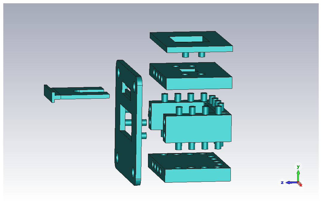
The new model not only allows for the originally intended improvement of conductivity, but also through division into planar components, smoothing with the 3D printer and thereby reducing surface roughness.
6.1 Simulation
The original WR90 model presented at the beginning is technically modified in a modular design, but still retains its basic form. The only modifications are the new addition of the cover to the flange and the removal of the old guide rails. As the model in the area of wave propagation has remained fundamentally the same, a new simulation of the S-parameters can be started directly by simply changing the conductor material to aluminum. The result of the new S-parameters differs little compared to the previous model with copper as shown in Fig. 12. This fact can be explained by the very good conductivity of aluminum with S m−1 (Kark, 2020) or according to the International Annealed Copper Standard (IACS) ≈64 % of copper conductivity.
6.2 Manufacturing
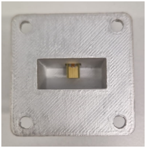
Due to the newly designed model and the now planar designed components, there is no longer a need for a specific orientation to avoid support structures in 3D printing. Furthermore, almost all internal surfaces are improved in terms of surface roughness, using the plug-in construction method, as mentioned earlier through the smoothing function. Following this the inner surfaces of the components will be sprayed with adhesive from the hardware store and coated with aluminum foil. Flanges and lids will be glued to the waveguide contact surfaces. The thickness of a layer of aluminum foil is approximately nine to eleven micrometers. To ensure a sufficient thickness of the conductor material this process is carried out at least twice for all components. During assembly the plug-in cylinders are carefully sprayed with glue and connected piece by piece. Once all parts are secured the prototypes are protected by cardboard and clamped in vices. After a sufficient resting period two additional coatings are applied to the outer sides of the new prototypes. This is intended to provide additional insulation against electromagnetic waves and improve transmission factors. Finally the coupling elements identical to those of the copper spray prototypes are reinstalled and fixed in the completed housing. A finished aluminum prototype according to the new concept is shown in Fig. 13.
6.3 Results
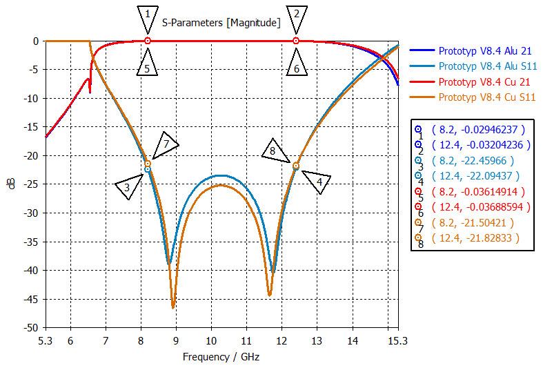
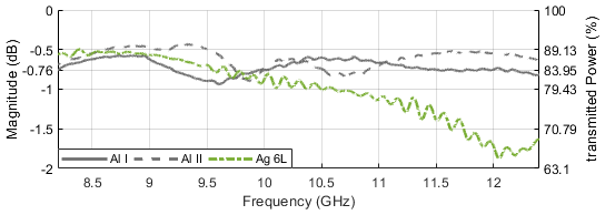
In order to compare the performances of the aluminum prototypes with those of the copper prototypes their S-parameters must also be extracted respecting the extraction method in Sect. 4.1 and the deembedding method in Sect. 4.2. For a better comparison with the already analysed copper prototypes their deembedded S-parameters are also revisited. The S11 parameters of both new prototypes are widely in the range of −15 to −25 dB as depicted in Fig. 14. Notably the prototype Alu II has a resonance peak in the frequency range of 9.5 GHz to approximately 10.5 GHz, which is better than −40 dB. According to the S11, the S22 parameters in Fig. 15 also mostly fall within −15 and −20 dB. An exception is the beginning of the frequency range where both prototypes exceed the −15 dB mark.
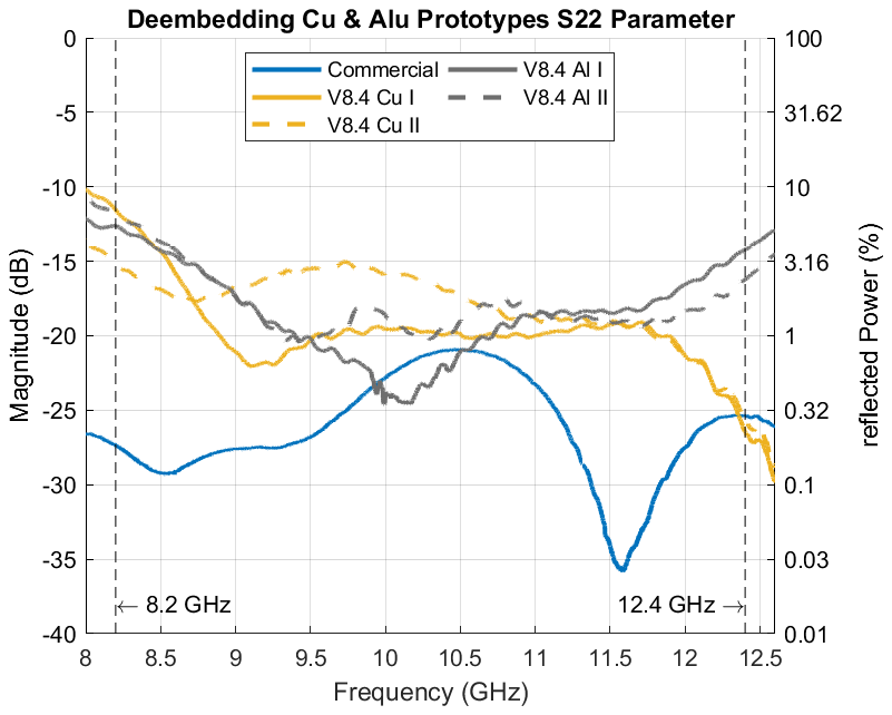
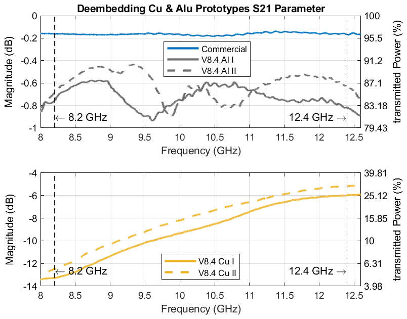
With observation of the transmission parameters in Fig. 16, a significantly better transmission for the aluminum prototypes can be immediately noticed. They all consistently exceed −1 dB and only differ from each other to a very slight degree. As can already be seen from the graphical classification within the logarithmic scale, the new concept results in a significant increase in performance despite the consistent SMA coupling elements. These observations are confirmed by the reflected powers of all waveguide ports of both prototypes as well, with values ranging between 1 % and 1.7 % according to Table 3.
Table 3Average S-parameters and Performances of the Aluminum Prototypes.
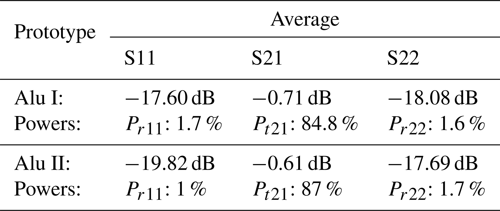
Causally responsible for the improvement of the reflection factors are mainly the better electrical contacting of the SMA coupling elements with the housing of the waveguide and the reduction of surface roughness by smoothing and gluing the aluminum, as well as the higher conductivity of the aluminum foil compared to the copper varnish. The remaining performance limitations still exhibit some inaccuracies in the material parameters and the manufacturing process. Thus, the coupling and reflections can still not be considered good, but certainly acceptable.
Similarly, according to Table 3, there is a significant increase in the power accepted, being within a range from 84.8 % to 87 % for both aluminum prototypes. In comparison to the commercial prototypes, with an average of 96 % power transmitted, this sample can already be considered viable. This clearly implies that, in contrast to the prior variant, the aluminum clad forms a feasible EM boundary, guiding a significantly larger portion of energy to the opposite port. It is also worth mentioning that the transmission parameters of the aluminum prototypes behave quite consistently across the entire frequency range, unlike those of the copper prototypes. This observation is confirmed for a DUT of the WR187 waveguide standard as well. Revisiting the mechanical construction, a lack of robustness is identified. In particular, the reflection at the input of the DUT is prone to mechanical stress which is unavoidable and introduced through bending of attached cable assemblies during measurement. A reinforcement and precise alignment, which can be provided by screw clamps, prevents parts of the assembly to loosen or even break. Improved mechanical stability leads to a better performance and increased reproducibility of measurements. Care should be taken to properly secure the SMA accessories, as almost any mechanical stress is inserted through the connectors into the structure. For the assembly presented in the following section, this drawback is taken into account.
To outperform the aluminum prototypes with approximately 90 % transmitted power, a further increase of the surface conductivity should be taken into account. In the group of relevant electrical conductors, we see in ascending order: aluminum, gold, copper, and silver. Besides the materials tested before, a simply applicable coating with good availability can be found in silver infused conductive paint. These are typically advertised to repair broken circuit board tracks or to directly form antennas on various surfaces. In the following test, the surface is finished with “L100 conductive Silver” provided by Kemo Electronic GmbH (Kemo L100 Data Sheet, 2024), as described below. This silver conductive paint is applied using a brush. Therefore, the initial single-piece design of the housing can be used without the necessity of separating it into various parts to access all surfaces. To achieve a homogenous distribution of the suspension, the handling information shall be strictly followed. All inner surfaces and contact areas of the transition body are coated with several layers of lacquer. The impact of the coating thickness is subject to intermediate measurements until a final number of twelve layers to form the electromagnetic boundary is reached. The finished prototype with the coupling element being inserted and locked is shown in Fig. 17.
7.1 Results
The S-parameters are again deembedded in the same manner as done before for the preceding DUTs. Tests with a surface coating thickness of three, six, nine, and twelve layers are conducted and considered in the final data analysis. As conductivity is expected to increase with the number of layers, its effect is covered by examining the measurements stepwise.
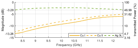
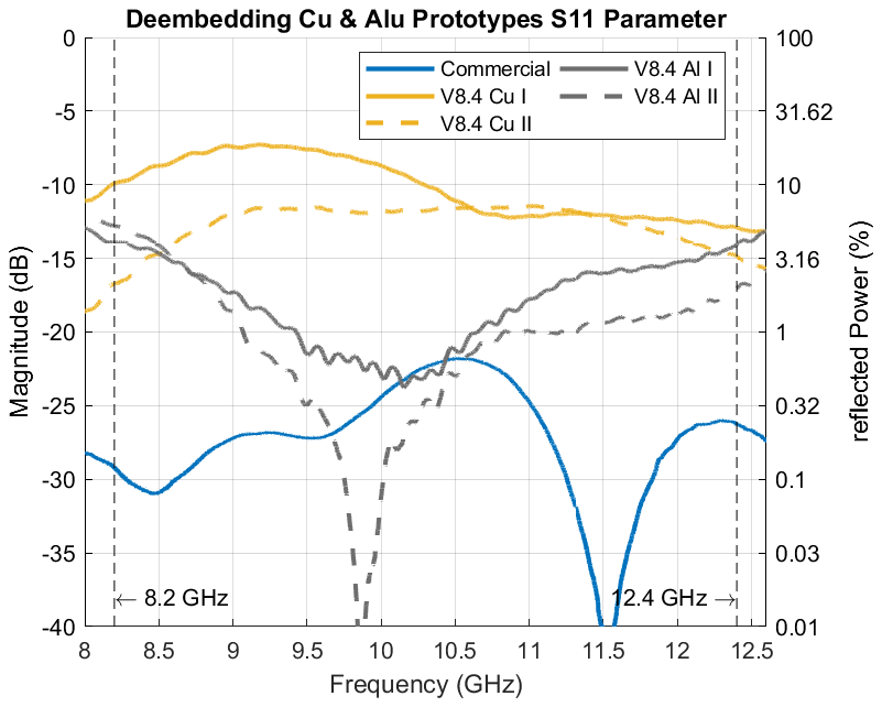
Figure 18 contains a comparison of the preceding Copper samples with a three-layer silver coated DUT, indicating a flattened frequency response and generally a better power acceptance in the range of around 50 %. This is indeed still far below the performance of the aluminum cladded sample which was at more than 80 % accepted power. With a total number of six silver conductive layers being applied, the transmission, as per Fig. 19, Ag 6L, is now close to the performance of the aluminum cladded samples, at least within the X band fraction between 8.2 and 10.5 GHz. Insertion loss rolls off to about 1.5 dB at 11.75 GHz.
In a direct comparison between WR90 and WR187 following the same silver coating approach, again better performance is observable for the lower frequency range waveguide of the G band (3.95–5.85 GHz) compared to the X band ranging between 8.2 and 12.4 GHz. The fact allowed for the inference of insufficient conductivity of the metallization, but in this case power transmitted at small frequencies already reaches more than 80 % so the argument cannot be made.
Instead the aspect dealing with the varying frequencies and constantly changing angles of incidence must be considered. The incoming wave splits at the interface boundary of the dielectric of the prototype and the metallization into a part reflected into the interior of the waveguide and a part transmitted into the metallization. If a high percentage of the incident wave is already reflected back into the prototype due to the high conductivity of the metallic coating, ultimately the angle of reflection dependent on the angle of incidence is responsible for efficient transmission of the wave. Due to the additive manufacturing as done for the copper coated sample, the same aspect might be considered here. Surface roughness is the suggested major limiting factor, correlating to the observation of lower performance at higher frequencies. An increased occurrence of reflections also results in additional wave components transmitting from the inside of the waveguide to the metallization, which also contributes to power loss.
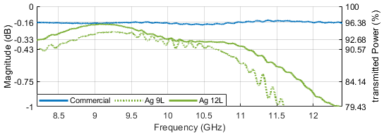
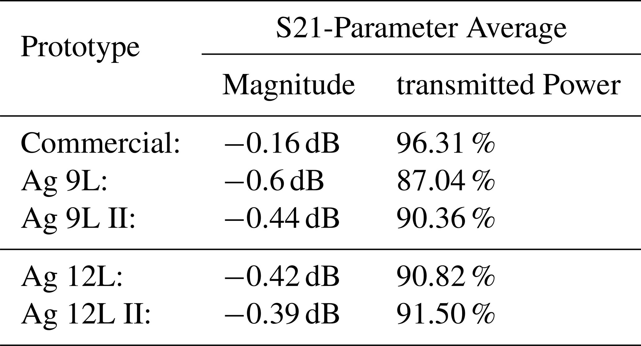
To further improve power acceptance in the upper frequency range, the closest approach is to further increase the number of coating layers. Besides an increase of the conductivity of the coating, with an increasing number of layers also the surface will be flattened as the lacquer tends to fill the gaps within the layers of the 3D printed base structure. Figure 20 clearly indicates the effect caused by the increased surface coating thickness: The nine layer and twelve layer variants prove that high frequency response correlates to surface thickness. In summary, the aluminum variant is outperformed by the silver coated DUT for frequencies up to 10.5 GHz when applying six layers (Ag 6L), up to 11.5 GHz when applying nine layers (Ag 9L), and up to 12.4 GHz for twelve layers (Ag 12L), which represents the uppermost frequency tested. While the transmission of aluminum and silver versions are quite comparable in magnitude, the silver version is significantly better in the low and mid-range X band. Here the 12-layer silver DUT competes with the commercial grade WR90 CWT. In Fig. 20, with more than 95 % power transmitted at 9.1 GHz, the benchmark of the industrial part is reached. When considering the entire frequency span tested, the arithmetic average of the DUT after deembedding calculates to more than 90 % of the power incident being available at the ouput, as summarized in Fig. 22 and Table 4.
In the following sections, the impact of different material parameters, properties and the design elements onto the performance of the waveguides are discussed for further consideration for the designing process.
8.1 Impact of Conductivity
Based on the theory of waveguides, the H10 fundamental mode of a hollow waveguide can be described by a TEM wave obliquely oriented in the hollow waveguide which is reflected onto the metallic side walls which are first assumed to be lossless (PEC) and which is superposing itself in the inner of the waveguide. Thus the H10 which has a sine dependency can be expressed by a superposition of two oppositely propagating TEM waves where the tangential components of the wave vector have a phase shift of π while the normal component is similar according to Eq. (2) (Kark, 2020).
Accordingly the behavior of the individual TEM waves at the metallic walls can be considered as oblique incidence on a flat interface between two media. It is important to consider the orientation of the electric field with respect to the plane of incidence. With the linearly polarized E-field in the y-direction of the H10 wave, the so-called s-polarization as defined by Kark (2020) is present. According to the definition found there, reflection can be described as
using the field wave impedances of the adjacent media denoted as Z1 and Z2.
The angles (θ1) and (θ2) define the incidence and transmission angles respectively. The angle of incidence θ1 can be estimated by the components of the wave vector, while the transmission angle θ2 is found by the law of refraction. Based on Eq. (4) (Kark, 2020) the definition of field wave impedances relies on the material constants of permittivity (ε), permeability (μ) and conductivity (κ) as well as the angular frequency (ω).
If one defines the wave impedances for air and an infinitely well-conducting metal, a reflection factor of can be calculated. The entire wave would remain within the waveguide if the conductivity of the metallic coating were ideal. Conversely without specifically addressing the angle of incidence and material parameters it can also be concluded that the reflected field components decreases as conductivity decreases. It is therefore power lost inside the waveguide. Where the outgoing field components ultimately remain after transmission depends not only on the conductivity, but also on the thickness of the metal layer. According to Eq. (5), a direct relationship between the conductivity (κ) and the skin depth (δ) of a wave in a metal can be established. Also the frequency (f) and permeability (μ) have an influence on the attenuation of the wave penetrating into the metal (Kark, 2020).
With decreasing conductivity, the wave emerging from the interior of the waveguide experiences weaker attenuation and can therefore, with a low or lacking thickness of the metallic layer, to a large extent reappear from the coating into the printed waveguide housing and then into the air. In addition to the usual losses due to heat also losses in the form of radiation could occur. When the wave exits the metallic coating, reflections and transmissions at the interfaces of metal-print and print-air must be taken into account. Furthermore in the case of completely missing or insufficient conductivity of the metallic coating, depending on the material parameters, aspects of total transmission and total reflection, which occur with different dielectrics, should also be considered.
Therefore the coating using copper spray can be declared as the main cause of extremely low transmission parameters S2,1 due to insufficient conductivity. Therefore an alternative metallic low-cost coating in the form of several layers of adhesive aluminum foil or silver ink is intended to ensure sufficient conductivity and layer thickness, so that better insulation of the advancing wave in the prototype can be guaranteed.
8.2 Impact of Surface Roughness
Surface roughness is an issue for 3D printed objects as the printed PLA lines are nearly cylindrical. Applying small wire diameters and by bringing these as close as possible to each other the surface roughness could be minimized from the beginning. Due to the temperature in the 3D print process the material exhibit a certain viscosity further reducing the surface roughness after cooling down.
The application of a paint with nano- or micro-structured metallization again reduces the roughness when hardening. The surface roughness is responsible for diffuse reflections as shown in Fig. 21. These can be flattened, thereby reducing their influence by eliminating additional wave propagation paths and unfavorable angles of incidence on reflection and transmission parameters as well.
8.3 Impact of SMA-Coupling Elements
Upon achieving sufficient transmission, the behavior of the prototype in connection with various coupling elements will now be examined. To do this, the fixed sliding cover must simply be loosened and another SMA coupling element must be inserted. Then using Fig. 22 and Table 4 the influences of different SMA coupling elements can be investigated based on the averaged transmission parameters. For example the use of an SMA coupling element manufactured in the same way as the previous one improves transmission parameters (Ag 9L II, Ag 12L II). This can be justified by the necessarily occurring geometric deviations caused by the manual production of the coupling elements.
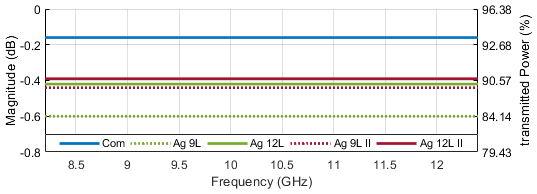
Table 4Average S-Parameters and Performances of the Silver Prototypes.
The performance analysis of the WR90 and WR187 copper prototypes suggests non-ideal manufacturing and metallization. Deviations in additive manufacturing, the production of the SMA coupling element using strip conductor technology and manual adjustments have a significant impact on the reflection factors.
The low transmission factors due to high metallic losses are related to the insufficient metallization. The results of the extracted S11 and transmission parameters of the prototype differ from those of the deembedded ones due to the assumed symmetry, but they can still be understood as “symmetrized averages” and therefore as a first approximation. The actual development shows that the method presented in Müller and Diewald (2015) is still valid for connector extraction with low transmission factors. The deembedding based on the extracted commercial CWT provides a very good reproduction of the individual prototype S-parameters according to performed reconstructions of the measurements M3.
Further, based on the modeling and simulation of the WR90 prototype, it is possible to adapt this model to even larger waveguide standards to improve the transmission. The results of the WR187 prototypes show improvements in both – reflection and transmission – parameters which are attributable to the influences of larger dimensions and lower frequencies which means lower losses. In line with the WR90 prototypes the differences between the simulated and commercial to the measured WR187 prototype S-parameters can once again be attributed to inaccuracies in manufacturing and insufficient quality of the copper spray.
Based on this, new prototypes are developed, constructed in a modular manner and covered with aluminum, and expected to significantly increase the performance of the S-parameters through reduced surface roughness and increased conductivity. With regard to the results of the deembedding, reflected powers with a minimum of 1 % and transmitted powers with a maximum of 87 %, the changes were crucial for a significant increase in efficiency. An application of the new prototypes would, without considering the aspect of instability, thus be fundamentally feasible in any case, but due to ongoing losses of more than 10 %, the presented concepts would still not be sufficient for applications with higher frequencies. Nevertheless a significant qualitative improvement of the prototypes originally metallized with copper spray can be achieved by using alternative conductor materials, in this case aluminum. Additionally by adjusting the manufacturing process based on the 3D models housing further causes of reflections and absorptions within the prototype can be corrected. Therefore, the deembedded S-parameters converges to those of the simulation S-parameters with an increase in conductivity and precision in manufacturing.
Ultimately further improvement by using a highly conductive silver paint allows the production of nearly industrial equivalent low-cost WR90 waveguide prototypes. The manufactured silver prototype transmits on average more than 90 % of the incoming power. Investigations of the deembedded transmission parameters in the higher frequency range and the effects of different coupling elements on the performances suggest an increasing occurrence of reflections. These are caused once more by unclean surfaces in additive manufacturing and inaccuracies in manual adjustment. These impact of this imperfections can be satisfactorily reduced in favor of the transmission parameters by applying additional layers of silver conductive paint. An option for more efficient optimization of surface roughness is offered by the concept of modeling as a plug-in kit consistently with that of aluminum prototypes. The perfection of manual craftsmanship is located outside of the possibility and therefore cannot compete with the results of a machine.
An alternative therefore is offered by the development of a coupling element that can dispense with the aspect of manual production and is already delivered ready-made. A potential approach to a specific application involves the use of a planar Vivaldi antenna, which can easily be inserted into a 3D-printed housing. This design is similar to a finline and has several advantages in modeling, simulating and production. Thus, the optimization of reflection parameters ultimately paves the way for ideal transmission parameters.
In this work no software code or additional data has been generated. The relevant design parameters are given in this publication. The Dassault CST MWS design files are not allowed to be shared due to restrictions of the educational license.
MF designed and implemented all waveguide structures, MF wrote the initial paper, SM processed the measurements for S-parameter extraction, SM reviewed the final paper. VL reviewed the final paper and gave fruitful hints for paper improvement, AD was responsible for conceptualization and project administration. AD gave access to the measurement technology.
The contact author has declared that none of the authors has any competing interests.
Publisher's note: Copernicus Publications remains neutral with regard to jurisdictional claims made in the text, published maps, institutional affiliations, or any other geographical representation in this paper. The authors bear the ultimate responsibility for providing appropriate place names. Views expressed in the text are those of the authors and do not necessarily reflect the views of the publisher.
This article is part of the special issue “Kleinheubacher Berichte 2024”. It is a result of the Kleinheubacher Tagung 2024, Miltenberg, Germany, 24–26 September 2024.
This paper was edited by Madhu Chandra and reviewed by Madhu Chandra and one anonymous referee.
Bialkowski, M. E.: Analysis of a coaxial-to-waveguide adaptor including a discended probe and a tuning post, IEEE Transactions on Microwave Theory and Techniques, 43, 344–349, https://doi.org/10.1109/22.348094, 1995. a
Calignano, F., Manfredi, D., Ambrosio, E. P., Biamino, S., Lombardi, M., Atzeni, E., Salmi, A., Minetola, P., Iuliano, L., and Fino, P.: Overview on Additive Manufacturing Technologies, Proceedings of the IEEE, 105, 593–612, https://doi.org/10.1109/JPROC.2016.2625098, 2017. a
Dewantari, A., Kim, J., Jeon, S., Kim, S., and Ka, M.: Tunable waveguide-to-microstrip transition for W-band antenna, IET Microwaves, Antennas & Propagation, https://doi.org/10.1049/iet-map.2018.5488, 2019. a
EMI35 Data Sheet: Kontakt Chemie, Technisches Datenblatt EMI 35, https://docs.rs-online.com/5d83/0900766b8159bea8.pdf (last access: 7 December 2025), 2024. a
Enayati, P. and Zarifi, D.: Design of a wideband coaxial-to-rectangular waveguide transition based on Supershapes, IEEE Access, 10, 121924–121929, https://doi.org/10.1109/ACCESS.2022.3222796, 2022. a
FMWCA1076 Data Sheet: Fairview Microwave, FMWCA1076 DATA SHEET, https://www.fairviewmicrowave.com/images/productPDF/ FMWCA1076.pdf (last access: 7 December 2025), 2024. a
FMWCA1107 Data Shee: Fairview Microwave, FMWCA1107 DATA SHEET, https://www.fairviewmicrowave.com/images/productPDF/FMWCA1107.pdf (last access: 7 December 2025), 2024. a
Goode, I. and Saavedra, C. E.: 3D printed linearly polarized X-Band conical horn antenna and lens, IEEE Open Journal of Antennas and Propagation, 3, 549–556, https://doi.org/10.1109/OJAP.2022.3173161, 2022. a
Helena, D., Ramos, A., Varum, T., and Matos, J. N.: The use of 3D printing technology for manufacturing metal antennas in the 5G/IoT context, Sensors, 21, 3321, https://doi.org/10.3390/s21103321, 2021. a
Kark, K. W.: Antennen und Strahlungsfelder, Elektromagnetische Wellen auf Leitungen, im Freiraum und ihre Abstrahlung, 8th Edn., Wiesbaden: Springer Fachmedien GmbH, https://doi.org/10.1007/978-3-658-38595-8, 2020. a, b, c, d, e
Kemo L100 Data Sheet: Kemo Electronic GmbH, Kemo Electronic L100 Conducting Silver Data Sheet, https://www.kemo-electronic.de/datasheets/l100.pdf (last access: 7 December 2025), 2024. a
Montejo-Garai, J. R., Marzall, L., and Popović, Z.: Octave bandwidth high-performance microstrip-to-double-ridge-waveguide transition, IEEE Microwave and Wireless Components Letters, 30, 637–640, https://doi.org/10.1109/LMWC.2020.3000283, 2020. a
Müller, S. and Diewald, A. R.: Methods of connector S-parameter extraction depending on broadband measurements of symmetrical structures, 2015 Loughborough Antennas & Propagation Conference (LAPC), 2015 11th, 1–4, https://doi.org/10.1109/LAPC.2015.7366144, 2015. a, b, c, d, e, f
Pérez-Escudero, J. P., Torres-García, A. E., Gonzalo, R., and Ederra, I.: A simplified design inline microstrip-to-waveguide transition, Electronics, 7, https://doi.org/10.3390/electronics7100215, 2018. a
Pozar, D. M.: Microwave Engineering: Theory and Techniques, USA, John Wiley & Sons, Incorporated, ISBN 978-1-119-77062-6, 2020. a
Santiago, D., Laso, M. A. G., Lopetegi, T., and Arregui, I.: Novel Design Method for Millimeter-Wave Gap Waveguide Low-Pass Filters Using Advanced Manufacturing Techniques, IEEE Access, 11, 89711–89719, https://doi.org/10.1109/ACCESS.2023.3305956, 2023. a
SC7505 Data Sheet: Fairview Microwave, SC7505 DATA SHEET, https://www.fairviewmicrowave.com/images/productPDF/SC7505.pdf (last access: 7 December 2025), 2024. a
Simone, M., Fanti, A., Lodi, M. B., Pisanu, T., and Mazzarella, G.: An in-line coaxial-to-waveguide transition for Q-Band single-feed-per-beam antenna systems, Applied Sciences, 11, 2524, https://doi.org/10.3390/app11062524, 2021. a
Waveguide Data Sheet: Millimeter Wave Products Inc., Waveguide Frequency Bands with Interior Dimensions, http://miwv.com/images/Waveguide-Chart.pdf (last access: 7 December 2025), 2024. a
- Abstract
- Introduction
- Simulation
- Manufacturing
- Measurements
- Method Applied on Larger Waveguide Standard
- Alternative Concept based on a Modular Design
- Silver Paint Surface Coating
- Discussion
- Conclusion
- Code and data availability
- Author contributions
- Competing interests
- Disclaimer
- Special issue statement
- Review statement
- References