 | 04 Sep 2018
Influence of an Electrically Non-Conducting Heat Sink for Power Semiconductors on Radiated Interferences
Kai Rathjen
Sebastian Fahlbusch
Klaus F. Hoffmann
Stefan Dickmann
Power semiconductors are used in a growing number of applications. Furthermore, faster switching transients and therefore higher switching frequencies can be realised. This leads to higher radiated interferences at higher frequencies. In power electronic applications, often a cooling concept for the semiconductors is required to comply with the allowed temperature range. Typically, heat sinks are made of aluminium and their conductive behaviour can cause EMC problems. Via capacitive coupling, voltage transients are transferred from the power semiconductor to the heat sink, so that the heat sink behaves as an antenna and radiated interferences occur. Furthermore, a common mode current will appear if the heat sink is grounded. In this paper, a promising approach to reduce radiated interferences from the heat sink and solve the common mode issue by using an electrically isolating ceramic heat sink is presented. The influence of an aluminium nitride ceramic heat sink on cooling performance and EMC behaviour has been investigated. For this purpose, two geometrical identically heat sinks made from aluminium and aluminium nitride have been compared regarding thermal performance and radiated interferences characterised by S-parameters.
- Article
(974 KB) - Full-text XML
- BibTeX
- EndNote


The development of modern power semiconductors, especially based on wide band gap materials like gallium nitride and silicon carbide, allows for steeper switching edges and therefore higher switching frequencies, which can be used to design more compact power electronic systems and systems with higher efficiency. However, these developments lead to rising radiated interferences at higher frequencies (Dolente et al., 2005; Kostov et al., 2013; Rong and Lin-Chang, 2002; Ryan et al., 2002). Furthermore, in most power electronic applications, a cooling is required due to the occurring losses. Despite of an electrical isolation between the heat sink and the power semiconductor, the heat sink can act as an antenna. The immediate vicinity of the heat sink to the switching operations in the power semiconductor leads to a capacitive coupling. Hence, voltage transients from the switching operations are transferred to the heat sink and cause radiated interferences. If the heat sink is grounded, an increased common mode current will occur.
The spectrum of the drain-source-voltage uDS of a SiC-MOSFET (1.2 kV, Wolfspeed, Cree Inc.) operating in switching mode used in a hard switching half bridge topology is exemplarily shown in Fig. 1 in frequency domain. Also shown are envelope lines with slopes of −20 and −40 dB decade−1. The details of the switching operation are 600 V input voltage, 15 ns turn-on time, 30 ns turn-off time and a switching frequency of 1 MHz. The spectrum shown in Fig. 1 was calculated using data from Fahlbusch et al. (2015). It gets obvious, that for the investigations regarding radiated interferences, frequencies up to 1 GHz have to be taken into account.
Heat sinks have been subject of electromagnetic compatibility (EMC) research for a long time. Many investigations are about prediction and optimisation of EMC based on the heat sink geometry, often using simulation techniques (Dolente et al., 2005; Ryan et al., 2002; Brench, 1994). Furthermore, the influence of grounding was investigated in different publications (Rong and Lin-Chang, 2002; Arien et al., 2015; Bhobe and Sochoux, 2008). Grounding can also cause EMC problems. It is a crucial problem especially for large heat sinks and high frequencies.
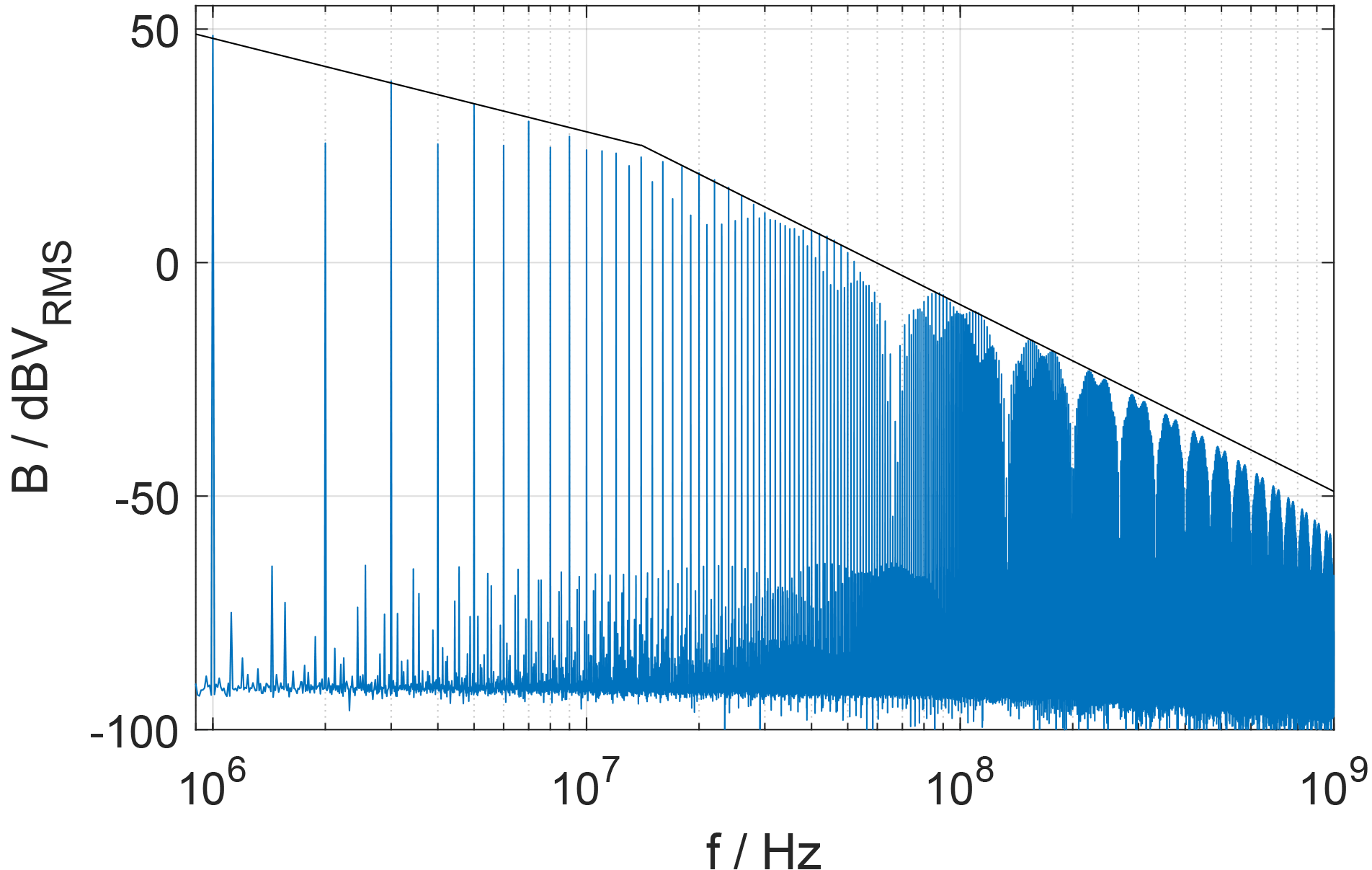
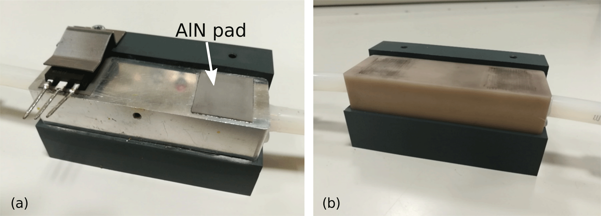
Figure 2Heat sink made from aluminium with MOSFET and two isolation pads (a); heat sink made from aluminium nitride (b).
A promising approach to reduce radiated interferences and to simultaneously solve the grounding problem is the utilisation of ceramic materials for heat sink designs. Particularly aluminium nitride, a sintered ceramic, exhibits high thermal conductivity of 180 W m−1 K−1 (for comparison: aluminium 236 W m−1 K−1) so that a sufficient cooling performance can be expected. Also the antenna effect of a heat sink made from aluminium nitride is reduced because of its very high specific resistance of more than 5×10¹⁰ Ω m.
In this paper, investigations about the thermal performance and the influence on radiated interferences of a heat sink made from aluminium nitride used for cooling power semiconductors are reported. For the investigations, a power semiconductor in the common TO-247 package was chosen. Two heat sinks of the same geometry were manufactured, one made of aluminium and one of aluminium nitride. To realise water cooling, both heat sinks have a 10 mm bore. They further feature a length of 90 mm to mount up to 4 TO-247-packages. The two heat sinks are shown together with a MOSFET in Fig. 2.
2.1 Thermal properties
The thermal resistance of the cooling system from MOSFET to cooling water is determined by the thermal resistances of the several components and the thermal resistance of the transitions between them. Schematics of the cooling system are shown for both heat sinks in Fig. 3. Using more than one MOSFET in a TO-247-package on the same electrically conducting heat sink, each MOSFET has to be isolated from the heat sink. This is because the contact area for heat dissipation of the MOSFET's package is not electrically isolated. It is connected to the drain potential and thus requires individual isolation when mounted on a shared heat sink. In this work, the isolation was done using 0.5 mm thin aluminium nitride pads, as shown in Fig. 2 on the left. Comparing the cooling system of aluminium and aluminium nitride heat sink, the isolation pads lead to additional thermal transition resistances in the aluminium heat sink system. The thermal resistance of the pad itself is nearly negligible. To minimise these transition resistances between MOSFET, heat sink and isolation pad, respectively, heat conducting wax was used as thermal interface material (TIM). Summing up the comparison of the two cooling systems, the aluminium heat sink exhibits higher thermal conductivity and therefore lower thermal resistance, but due to electrical isolation there is an additional thermal transition resistance within the additional TIM.
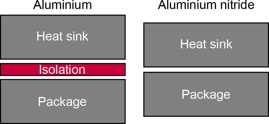
Figure 3Scheme of cooling system using aluminium and aluminium nitride heat sink, respectively.
Experimental investigations on the thermal performances of the heat sinks were done by cooling two SiC-Power-MOSFETs (C2M0080120D, Wolfspeed, Cree Inc.) within a half bridge topology. While there was a positive gate-source-voltage uGS applied, a drain-source-current of 20 A was used to generate dissipation losses due to the drain-source-resistance of the MOSFET in on-state RDSon. The package of the respective MOSFET was observed by an infrared camera during the experiment. Over time, uGS was reduced stepwise to increase RDSon. The mean temperature difference between the package and cooling water temperature using the aluminium nitride heat sink was ΔT=29.8 K and ΔT=34.0 K with the aluminium heat sink. Therefore, using the aluminium nitride heat sink, the temperature difference ΔT was 12 % less. Considering the measurement uncertainty, the aluminium nitride heat sink exhibits at least the same thermal performance compared to the aluminium heat sink.
2.2 S-Parameter
Concerning the EMC properties, S-parameters were measured in a semi-anechoic chamber. The DUT was placed on a grounded metal plate within the chamber. For the investigations, a replication of a TO-247-package was used, which is shown in Fig. 4 together with a scheme of the measurement setup. The TO-247-replication is to replicate the package contact area which is on drain potential, when a MOSFET in TO-247-package is used with a heat sink. Due to switching operations, rapid potential changes relative to ground occur at the area for heat dissipation.
An SMA feedthrough in the grounded metal plate is used to connect the TO-247-replica to port 1 of a network analyser (VNA). The TO-247-replica was directly soldered on the signal pin of the SMA feedthrough. For the S11 measurements, full calibration of VNA's port 1 was carried out regarding the end of the measurement cable connected to the SMA feedthrough. A manual SMA calibration kit featuring open, short and match was used. The shield of the measurement cable was grounded at its both ends: At the one end through a connection to the chamber wall, at the other end through the SMA feedthrough in the grounded metal plate. Furthermore, a test during the measurements on current flowing through the shield was negative.
To port 2 of the VNA, a log-per antenna was connected which was 3 m away from the DUT. For the S21 measurements, forward calibration of the VNA from port 1 to port 2 was applied regarding the ends of the measurement cables. Two manual calibration kits were used, SMA for the measurement cable to the DUT, N-type for the measurement cable to the antenna. The following test scenarios were investigated using the above described measurement setup:
-
MOSFET-replica without heat sink – “Without heat sink”
-
Aluminium nitride heat sink – “AlN”
-
Aluminium heat sink not grounded – “Al floating”
-
Aluminium heat sink grounded – “Al grounded”
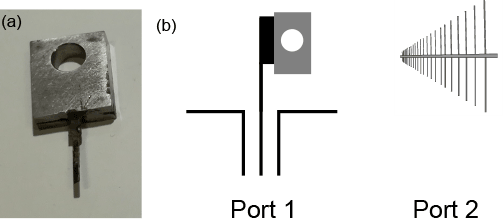
Figure 4Replication of TO-247-package (a), schematic of measurement setup for S-parameters (b).
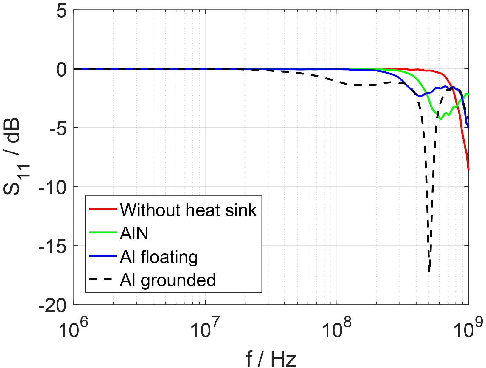
The measurements concerning parameter S11 are shown in Fig. 5 as magnitude in dB for the frequency range of 1 MHz to 1 GHz. Using this type of diagram, 0 dB corresponds to total reflection and negative values to unreflected power, respectively. Apart from the resonances above 300 MHz, which appear due to geometry of the measurement setup, there is nearly total reflection occurring.
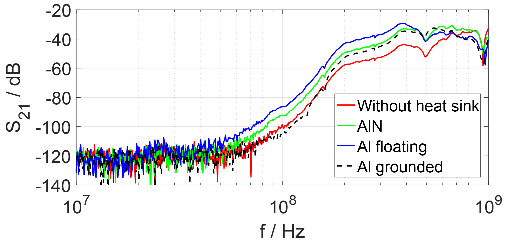
Besides the measurements of S11, measurements of S21 were carried out as well. The data regarding S21 are shown in Fig. 6 as magnitude in dB for the frequency range from 10 MHz to 1 GHz. Below 30 MHz the measurement signal was under the detection limit. From 30 MHz to approx. 300 MHz, the data show a uniform rise, while above 300 MHz resonances are visible, which can be probably attributed to the geometry of the measurement setup. The measurements are confirmed qualitatively by a simulation using the FIT method. Regarding the test scenario without heat sink and with aluminium heat sink, the measuring results confirm our expectations. “Without heat sink” and “Al grounded” behave similarly, because of the grounding the aluminium heat sink did not contribute to radiated interferences up to 150 MHz. Therefore, only the TO-247-replica was emitting. If the aluminium heat sink is not grounded, it will lead to higher radiated interferences. The emission of the aluminium nitride heat sink is in between “Al grounded” and “Al floating”. The comparison of “AlN” to “Without heat sink” shows that the aluminium nitride heat sink increases the radiated interferences. This effect will be discussed in the following paragraphs.
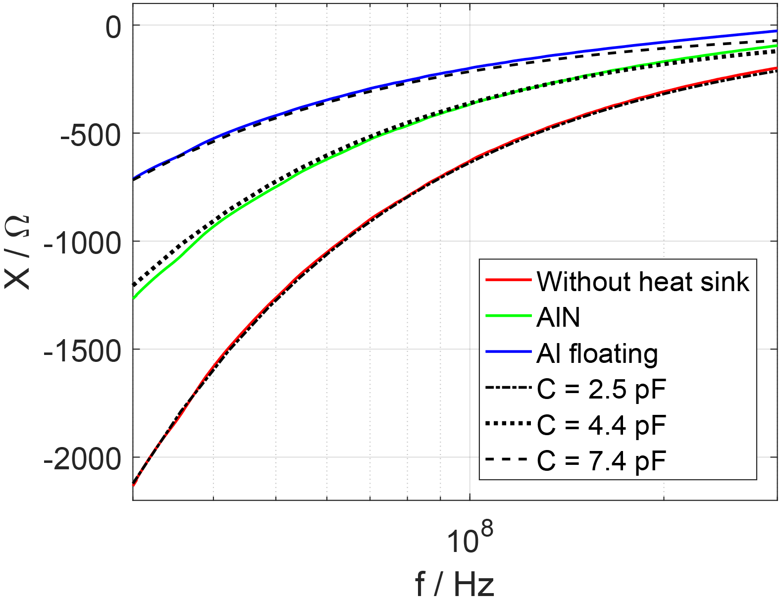
In order to understand why the aluminium nitride heat sink leads to more radiated interferences in comparison to the grounded aluminium heat sink, the TO-247-replica was considered as an antenna with the impedance . The antenna resistance RA represents the losses and the radiation resistance. In the frequency range below the resonances, the antenna can be considered as a short monopole, so that RA≪XA Fujimoto and Morishita (2013). This is possible in this frequency range, because the wavelength is much greater than the MOSFET and heat sink dimensions, respectively, and due to the S11 smith diagrams. Furthermore, for this relatively low frequencies, we do not expect high amount of losses in RA. A short monopole is considered to be capacitive Fujimoto and Morishita (2013). The reactance XA of the antenna, which is dominant for the frequencies of interest here, could be calculated from the data of S11. The reactances of the test scenarios “Without heat sink”, “AlN” and “Al grounded” are shown in Fig. 7. The capacitive behaviour of the DUT is obvious, so that reactances based on capacitance values are fitted to the measurements. The capacitance rises from “Without heat sink” with 2.5 pF via “AlN” with 4.4 pF to “Al floating” with 7.4 pF. The rise of the capacitance from “Without heat sink” to “AlN” by a factor 1.8 is due to the dielectric properties of AlN. In both test scenarios the MOSFET-replica is the antenna. The higher capacitance of “Al floating” is because now the heat sink is the antenna. The geometry of the aluminium heat sink leads to a higher capacitance compared to the MOSFET-replica. Calculating the reactance using a formula given by Schelkunoff (1952), a similar behaviour can be found.
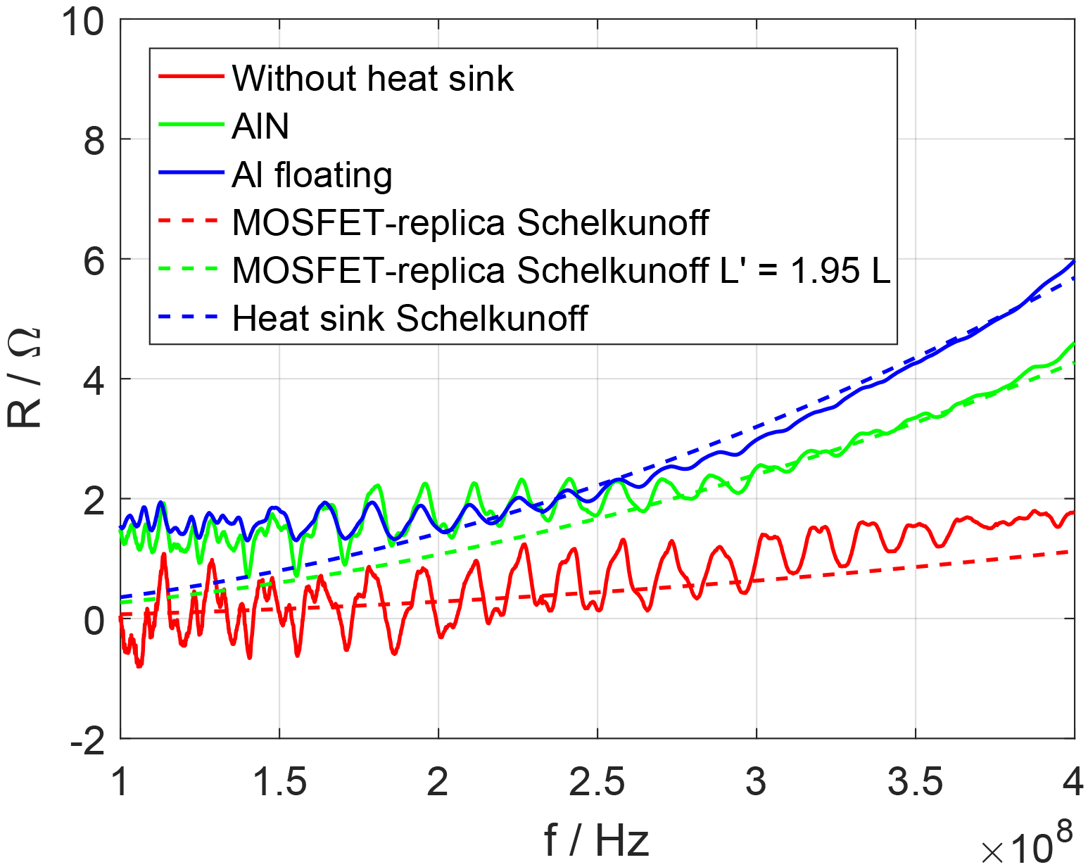
The radiation resistance RS, which is included in RA, is very small. Because it rises with the square of frequency, Schelkunoff (1952), for low frequencies, it is difficult to measure. In Fig. 8, the resistance of the antenna which was also calculated from S11 data is shown for the frequency range of 100 to 400 MHz. To show the frequency-square dependency of RS, a linear frequency axis was chosen. Below 200 MHz, RS does not reach the detection limit. Above 200 MHz, the frequency-square behaviour is visible. Furthermore, the radiation resistance was calculated using following formula from Schelkunoff (1952) for a short antenna above perfect ground,
with l length of the antenna and λ wavelength. For the wavelength, the vacuum wavelength was assumed using with c0 as speed of light in vacuum. The calculated values of RS are shown in dashed lines. The red dashed curve was calculated using the length of the MOSFET-replica. The green dashed curve was fitted to the “AlN” data using the length L as parameter. This led to an effective length L′ of the MOSFET-replica when mounted on the dielectric aluminium nitride heat sink. The dashed blue line was calculated using the heat sink geometry. The factor between the length L and the effective length L′ of 1.95 nearly fits the factor of 1.8 between the capacitances in Fig. 7 of “Without heat sink” and “AlN”. The good agreement between the measured and calculated data proves, that the assumption of a short monopole is applicable.
To understand the behaviour regarding to the aluminium nitride heat sink concerning the radiated interferences, the reflection factor r was considered. When the DUT is passive, the reflection factor from Strauss (2016)
with R0=50 Ω system resistance can be used. From Fig. 8 it is obvious, that RA is small compared to R0. Therefore, the reactance (Fig. 7), which has much higher absolute values, has a major influence on the reflection at the antenna input. The part of a signal, which is reflected at the input of the antenna, cannot reach the MOSFET and therefore it cannot contribute to radiated interferences. The reduction of the antenna reactance absolute value leads to a rise of radiated interferences because the alignment of the antenna to the input impedance is improved. The reason for the higher capacitance and lower reactance of the antenna, respectively and therefore lower reflection at its input using aluminium nitride is its relative permittivity of approx. 9. Of course, the intensity of this effect depends on the system impedance. In power electronic systems, a value of 50 Ω is rarely used as input impedance regarding the MOSFETs.
In this paper, an electrically non-conducting aluminium nitride ceramic heat sink was compared to a common aluminium heat sink. Both heat sinks were designed for use with water cooling. It was demonstrated, that the aluminium nitride heat sink exhibit at least the same thermal performance as the heat sink made from aluminium. The advantages of the aluminium nitride heat sink are the much lower leakage current to earth because the ceramic heat sink does not need to be grounded. This can save mass, assembly space and cost regarding to the line filter. For instance, for compact power converters based on gallium nitride, a lower leakage current to earth could be a major advantage. This is because in these converters for the line filter due to the common mode chokes, more space and mass is needed than for the power electronics itself. Furthermore, it is not necessary to apply an isolation between the heat sink and the MOSFET. On the other hand, a comparison between the aluminium and aluminium nitride heat sinks has shown that depending on the system impedance, the use of aluminium nitride heat sink can lead to higher radiated interferences. Also the manufacturing costs of ceramic heat sinks are much higher and there are manufacturing limitations regarding to the geometry. In summary, the aluminium nitride heat sink is an interesting approach for systems which need to be optimised strictly concerning mass and assembly volume.
Due to licensing restrictions, not all data can be made publically available. For scientific and non-commercial purposes, the data may be accessed via the corresponding author.
The authors declare that they have no conflict of interest.
This article is part of the special issue “Kleinheubacher
Berichte 2017”. It is a result of the Kleinheubacher Tagung 2017,
Miltenberg, Germany, 25–27 September 2017.
Edited by: Frank Gronwald
Reviewed by: Mathias
Magdowski and one anonymous referee
Arien, Y., Dixon, P., Khorrami, M., Degraeve, A., and Pissoort, D.: Study on the Reduction of Heatsink Radiation by Combining Grounding Pins and Absorbing Materials, Proceedings of 2015 IEEE International Symposium on Electromagnetic Compatibility (EMC 2015): [joint conference with EMC Europe]; Dresden, Germany, 16–22 August 2015. a
Bhobe, A. U. and Sochoux, P.: A Study of Grounded-Heatspreader for EMI Mitigation of ASIC IC Package, Proceedings of 2008 IEEE International Symposium on Electromagnetic Compatibility: [2008 IEEE EMC]; Detroit, MI, 18–22 August 2008. a
Brench, C. E.: Heatsink Radiation as a Function of Geometry, Proceedings of Compatibility in the loop: Chicago 1994; IEEE International Symposium on EMC, OCLC: 180504054, 22–26 August 1994. a
Dolente, A., Reggiani, U., and Sandrolini, L.: Comparison of Radiated Emissions from Different Heatsink Configurations, Proceedings of VI International Symposium on Electromagnetic Compatibility and Electromagnetic Ecology, 21–24 June 2005, Saint-Petersburg, 2005. a, b
Fahlbusch, S., Mueter, U., and Hoffmann, K.: Analysis of SiC-MOSFETs utilised in Hard Switching Inverter Topologies with Switching Frequencies up to 1 MHz, PCIM Europe 2015, Nuremberg, 19–21 May 2015. a
Fujimoto, K. and Morishita, H.: Modern Small Antennas, Cambridge University Press, New York, 2013. a, b
Kostov, K., Rabkowski, J., and Nee, H.-P.: Conducted EMI from SiC BJT Boost Converter and its Dependence on the Output Voltage, Current, and Heatsink Connection, 2013 IEEE ECCE Asia Downunder, 2013. a
Rong, L. and Lin-Chang, Z.: Heatsink grounding effect on radiated emission of electronic device, 2002 3rd International Symposium on Electromagnetic Compatibility, 2002. a, b
Ryan, N. J., Chambers, B., and Stone, D. A.: FDTD modeling of heatsink RF characteristics for EMC mitigation, IEEE T. Electromagn. C., 44, 458–465, https://doi.org/10.1109/TEMC.2002.801759, August 2002. a, b
Schelkunoff, S. A.: Antennas, Theory and Practice, 1st edition, John Wiley & Sons, Inc., New York, 1952. a, b, c
Strauss, F.: Grundkurs Hochfrequenztechnik, Eine Einführung, 2nd edition, Springer Fachmedien Wiesbaden, 2016. a