 | 19 Sep 2019
Inkjet printing of metal nanoparticles for green UHF RFID tags
Bruna Cruz
Andreas Albrecht
Philipp Eschlwech
Erwin Biebl
UHF RFID tags are nowadays widely and successfully implemented in many distinct applications, but unfortunately the traditional production process and incorrect disposal of such devices have a negative impact on the environment. In this work silver and gold nanoparticle inks were printed by a consumer inkjet printer on eco-friendly substrates like paper and PET in order to make the manufacturing process less harmful to the ecosystem. A dipole antenna with matching loop was designed for the RFID chip EM4325 from EM Microelectronics, which has an integrated temperature sensor, at the frequency of 866 MHz. Based on this design, simulations of the greener tags are presented and compared as a proof of concept, without optimizing the designs at first for the different materials. The printings with silver (unlike the gold) were conductive with self-sintering. IPL sintering was conducted to reduce the sheet resistance from the silver ink and to turn the gold ink conductive. First S11 parameter and read distance measurements are shown as well as the simulations with the optimized antenna designs.
- Article
(4653 KB) - Full-text XML
- BibTeX
- EndNote


Sustainability has become a development priority of modern industrial nations over the past years, going even so far, that information and communication technologies are traditionally viewed to have a negative impact on the environment. Radio Frequency Identification (RFID) as part of this technological branch has earned a comparable reputation. Most of RFID tags are neither biodegradable nor recyclable. On the other hand, from the integration of sensor technology to tags, RFID presents new opportunities in many industrial applications and can play an important role in applications helping to deliver a greener world. This can be observed by RFID circuits being used to improve green applications aiming for energy efficiency, waste reduction and recycling. Some of the ecological problems presented by today's RFID implementations are very evident. After all, the most important parts of an RFID tag, the IC and its antenna, include silicon and metallic components that are not compostable. Moreover, most RFID tags are housed in plastic or other petrochemical based materials. To combat this situation, some solutions can make the process less harmful to the environment, such as the use of paper as substrate, a material which is considered one of the best dielectrics for cheap and renewable microwave applications and it is environmentally friendly and compostable. Another alternative for the substrate, is the PET (Polyethylene terephthalate), which can be recycled. Additionally, new printing techniques like Inkjet printing are being used as a greener solution. Inkjet printing is a contactless process that is almost free of chemical waste and it doesn't require special facilities to be performed. Furthermore, the possibility of using well known substrates like paper films enable flexible, cheap, and disposable devices. While traditional methods to produce conductive patterns involve lithography, a multi-step subtractive process that is incompatible to roll-to-roll production, requires clean room facilities and produces chemical waste, additive printing methods like Inkjet Printing, promise high throughput, low-cost and improved environmental-friendliness. For this printing method, metallic inks containing gold, silver, copper and other metals, offer a much higher conductivity than polymer-based inks. Nobel metals are typically dispersed in solvents as nanoparticles to reduce their melting point. The use of metals as nanoparticles is a progress towards a greener solution, but they need to be dissolved in potentially toxic solvents. An alternative for that issue is the use of water based gold ink, so that all components of the ink are not dangerous for the ecosystem. The combination of those solutions can provide greener devices in order to reduce the impact of the traditional manufacturing techniques in microwave circuit design. This paper analyses the performance of the tags, inkjet printed on paper based substrate and PET utilizing gold and silver nanoparticles as ink.
A basic RFID system consists of a tag, a reader and a host system. The communication between an RFID tag and the reader/interrogator is realized by radio frequency (RF) waves. This technology enables data storage in small electronic transponder circuits that are particularly portable. In consequence, the stored data can be read and written without contact and often through obstructions. Those features enable many applications for RFID-based sensors. Currently, RFID systems are ubiquitous and extremely important by offering potential benefits in object identification and tracking in diverse application areas.
In order to implement these concepts, issues such as miniaturization, conformal and flexible materials, low power, low cost, mass production and environmentally friendly, passive or battery-less operation are fundamental. They lead to critical technological as well as circuit and system design challenges. This technology can be separated in a plurality of categories, each one able to address a suitable subset of the sought after features for applications and specification. One can classify RFID systems based on the type of electromagnetic interaction into near-field and far-field, or otherwise based on their operating frequency and corresponding operating standard. The most important frequency ranges for RFID systems are therefore, LF (100–135 kHz), HF (13.56 MHz) and UHF (865–868 MHz in Europe and 915 MHz in the US). In this paper the European UHF frequency range was considered.
Another important classification of RFID systems is based on their functionality, and divides them into passive, semi passive and active tags. Passive tags utilize the transmitted power from the reader to power their circuitry and to communicate with the reader. Semi passive tags utilize an additional power source, a battery, to power-up their circuitry, however, communication is still done passively, by reflecting or scattering the reader signal which arrives at the tag terminals. Active tags utilize an auxiliary power source to both power their circuitry and amplify and transmit back the incoming signals from the reader.
2.1 Passive tags
Passive tags rely on the transmitted power from the reader to both power their circuitry and communicate a response back to the reader. As a result, the operating range of such systems is limited by the minimum required power to operate the tag circuitry, rather than the sensitivity of the reader (Dobkin, 2008). The main challenge therefore becomes the minimization of the dissipated power of the tag circuitry as well as the maximization of the efficiency of the conversion from the electromagnetic power transmitted by the reader into electrical DC power used by the tag. Furthermore, the inclusion of sensing capability may further reduce the operating range of passive RFID systems, due to the additional power dissipated by the sensor circuits. However, the fact that no extra power is used to transmit data, allows for the implementation of a greener way of communication.
2.2 RFID green solutions
An important theme which is at present the focus of ongoing research efforts, is how technologies can be eco-friendlier, to avoid harming the environment. RFID is above all an information and communication technology. Therefore, it is viewed as having a negative impact on the environment. Moreover, RFID tags are neither biodegradable nor recyclable (Duroc and Kaddour, 2012). However, even if RFID is not an eco-friendly technology itself, from the integration of sensor technology into tags, it presents new opportunities in many industrial applications and can play an important role in applications helping to deliver a greener world. RFID circuits are being used to improve green applications aiming for energy efficiency, waste reduction and recycling, as outlined in the articles from Arebey et al. (2010) and Delen et al. (2011).
3.1 Inkjet printing
Inkjet printing is a digital and non-contact technique that is almost free of chemical waste and doesn't require special facilities to be performed. Furthermore, the possibility of using well known substrates like paper or polymer films enables flexible, cheap and disposable devices. It is ideal for fast prototyping and promise high throughput, low cost and improved environment-friendliness (Albrecht et al., 2016).
The main advantage of inkjet printing is its digital nature that allows every single printed drop and each pattern to be independent of the previous one. This means a high control over the process and no changeover costs if the same ink is used, making inkjet printing the cheapest printing technique for low volumes and thus it is often used in research. Furthermore, it is easily scalable using the same print head mounted on a larger stage or using multiple print heads.
Therefore, inkjet printing has gained a growing interest in many areas. Consumer desktop printers mainly use inkjet printing because it is a low-cost, reliable, quick and convenient method for printing digital files. Especially in the academic field, inkjet printing has gained a lot of interest in recent for electronics, life sciences, optics and coatings. Electronic components such as conductive lines, antennas, organic light emitting diodes, organic solar cells, organic field effect transistors, sensors, detectors and many more have been realized by inkjet printing (Cummins and Desmulliez, 2012).
3.2 Inks
Inkjet printing requires the functional material to be in a liquid form with restrictions on the viscosity and surface tension. To form a layer after printing, the material needs to contain or be converted to a solid material. The percentage of functional material in the ink controls the layer thickness of a single print and the number of printing cycles to achieve the desired thickness. The values are typically given as the solid loading, the ratio of the weight of functional materials to the weight of the ink. Common metal nanoparticle inks have solid loadings between 20 wt % and 60 wt % (Albrecht, 2018).
Water-based gold (Au) nanoparticle ink and silver (Ag) nanoparticle ink were used to print a set of prototype RFID transponder antennas.
3.2.1 Gold ink
The gold nanoparticle inkjet ink Au-LT-20 was purchased directly from the producer Fraunhofer ITKS (Dresden, Germany) from lot Au059. It contains 19.6±0.5 wt % gold nanoparticles dispersed in water having a viscosity of 7.3 cP at 22 ∘C and a surface tension of 35.1 mN m−1. The recommended curing temperature lies at above 150 ∘C and is optimized for adhesion on PET and polyimide. From the manufacturer information sheet, the particle size is limited to 200 nm. However, we measured a particle size of 20 to 40 nm as can be seen in the SEM image in Fig. 3. Still, a 400 nm filter should be employed while filling the cartridges. According to the manufacturer, the ink presents no harm to the eco system, it is nontoxic and biocompatible.
3.2.2 Silver ink
The used silver nanoparticle ink is DGP 40LT-15C from Advanced Nano Products (Sejong, Korea). The ink contains 30 wt %–35 wt % silver nanoparticles of around 50 nm diameter that are dissolved in triethylene glycol monoethyl ether (TGME) that has a high boiling-point at around 250 ∘C according to the Open Chemistry Database. The viscosity of the paste ranges between 10 and 17 cP depending on the temperature and age of the ink. The surface tension lies between 35 and 38 m Nm−1 according to the datasheet of the manufacturer. The ink can be washed with polar solvents, e.g. ethanol before drying and features a good adhesion after drying. The ink can be directly filled into printer cartridges after shaking it by hand. The colour of the ink is almost dark black with a slight green-brown tendency. The curing temperature lies between 120 and 150 ∘C leading to a specific resistivity as low as 11 µΩ cm according to the datasheet of the manufacturer.
3.2.3 Ink conductivity
Widespread conductive inks usually consist of dissolved or suspended metal nanoparticles. In order to enhance conductivity of a printed structure, a drying and sintering process is needed to remove binders or organic stabilizers from the ink (Wunscher et al., 2014). Sintering is usually done by heating or pressuring the printed conductive elements to a high temperature without melting them to form a compact mass of nanoparticles. After the stabilizers are removed the nanoparticles can coalesce at the particle interface and form a conductive path.
Once the antenna is printed and sintered, the sheet resistance and the thickness of the film can be measured and the resistivity can be obtained from Eq. (1):
where Rs is the sheet resistance, t is the thickness and ρ is the resistivity. Equation (2) shows that with ρ one can calculate the conductivity σ of the printed film since the conductivity is the inverse of resistivity:
The thickness and sheet resistance obtained from the printed films are discussed in Sect. 6.1.
3.3 Substrates
The possibility of implementation of inorganic materials such as PET and organic materials such as paper can lead to a manifold of advantages. It is proven that organic substrates have lower cost and are easily biodegradable. This makes them a promising material for the realization of eco-friendly electronics.
3.3.1 Paper as substrate
Paper is a promising substitute for plastic substrates. It is considered one of the best dielectrics for cheap and renewable microwave applications. It is environmentally friendly and compostable. It can undergo large reel to reel processing which makes it a very suitable material for cheap mass production and it allows for the use of direct write technologies like inkjet printing.
Paper substrates have a relative permittivity (εr) between 2.8 and 3 and the loss tangent (tan δ) is around 0.05–0.06.
The 200 µm thick paper based substrate used in this work is the “Emblem WAPUM Glossy 240g” from Dataplot.
3.3.2 PET
Polyethylene terephthalate (PET) is a flexible substrate material used for many applications in electronics since it is inexpensive and has good mechanical and electrical properties. Additionally, what make it of such value in this work, it is that it can be recycle. PET has a relative permittivity (εr) of 3.4 and its tan δ is 0.002.
A 150 µm film polymer based substrate “Reprofilm HD” from ColoGATE was utilized.
In a RFID system, a tag antenna acts as a power receiver that transforms the emitted electromagnetic wave into electrical energy for the chip, as well as a radiating source that sends out digital information embedded inside the chip. For the purpose of energy conversion, the tag chip includes a charge capacitor that causes the tag chip to have largely reactive characteristic impedance, making the antenna more difficult to match with the tag chip than with a general radio frequency system of 50 Ω characteristic impedance. The electromagnetic power from the antenna is maximally delivered to the tag chip when the antenna has a complex conjugate impedance of the chip, that is , where Zc is the chip impedance and Za is the antenna impedance (Finkenzeller, 2010). Since the energy transfer between the chip and antenna is the most important issue, a successful antenna design is determined by conjugate impedance match between both components.
4.1 Folded dipole with closed loop
Dipole antennas are widely used in UHF RFID. They have a simple single-layer structure fit for label type tags. Moreover, the dipole antenna radiation pattern is omnidirectional in the plane perpendicular to the dipole axis. Compared with directive antennas, this provides broader spatial coverage for power harvesting. Size-reduction techniques for dipole type antennas are also well-established. Dipole tag antennas can provide sufficient platform-tolerance to guarantee the reliable identification when mounted on most dielectric objects with low permittivity.
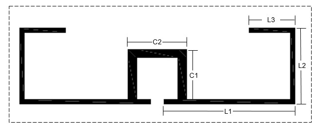
The chosen antenna design is a folded dipole with a closed loop near the tag chip for impedance matching. The required input resistance (Ri) and reactance (Xi) can be achieved separately by choosing appropriate geometry parameters. This allows the antenna to match to the to tag chips that usually have small resistance and large reactance. The folded dipole provides great freedom for impedance adjustment especially for the imaginary part, which is a very important feature for conjugate impedance design. This is achieved by tuning geometry parameters L1, L2 and L3 shown in Fig. 1 (Qing and Yang, 2004). After obtaining a satisfactory imaginary part, the closed loop is added to the previous folded dipole antenna and it tunes the geometry parameters C1 and C2 for the required conjugate impedance. The closed loop makes impedance matching easier, especially when small resistance parts of the antenna impedance are required.
4.2 Design
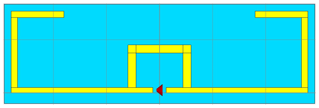
The dipole antenna with matching loop was designed with CST Studio Suite to match the RFID chip EM4325 from EM microelectronics. At the resonance frequency of 868 MHz, the impedance of the chip is Ω. This RFID chip has an integrated temperature sensor, which fits in the green concept of this work. Less additional circuit to build means that less material has to be used.
First an antenna for copper on FR4 as substrate was designed and a prototype was realized with etching technique for further comparison. This technique is commonly used in the manufacture of circuit boards and it brings good technical results, but in contrast, it has many negative consequences for the environment, once there are a lot of materials waste and acids are used in the etching process. With this prototype (Fig. 2), standard RFID tests such as read distance and resonance frequency were made in order to get a reference measurement to compare with the “green” tags.
The same pattern was used to make the other prototypes using inkjet printing technique, not optimized for the specific substrate and ink at first, just to compare performance regarding read distance.
A low cost consumer inkjet printer, the Workforce 2010W by Epson, was used without further modification for the printing of the samples as shown in Fig. 3. Since the print resolution was not an issue due to the width of the antenna's arms and the substrates were flexible enough to be bent in the paper feed, a high resolution printer was not necessary, enabling the advantage of a faster printing speed. The four colour printer has 180 nozzles for the black ink and 59 nozzles per colour, which are equally placed in two rows on a one-inch long nozzle plate. The resulting distance between the nozzles is 141 µm with a nozzle diameter of 25 µm. The resolution of the printer is 5760 × 1440 dpi and the minimum droplet size is 3 pl. The printing of an A4-sized page takes less than a minute and forms a homogeneous wet film on non-absorptive substrates.
The black cartridge was replaced by a refillable cartridge filled with gold or silver nanoparticle inks and the colour cartridges were filled with distilled water or ethanol. The gold ink was filtered with a special filter recommended by the manufacturer and dissolved in water for a better resolution. The silver ink was used without processing except for shaking prior to filling the cartridge. It's worth pointing out that a prototype was printed with a professional laboratory scale inkjet printer DMP-2831 of Fujifilm Dimatix Inc as well. In spite of the printer high-precision characteristic, the resolution of the sample using the gold NP ink was not ideal and it took four hours to print one layer.

Before printing the samples, the nozzles were cleaned and it was assured that no nozzles are blocked or misfiring because of air within the channels. The samples were printed with the regular printer driver and the settings Epson Matte and the quality setting Strong. A finer raster and slow printing were used. The paper and PET were fed through the built-in paper feed. Often, the inkjet-printed film does not have the desired functionality directly after printing and some post-processing treatments are necessary to achieve it. Due to the high solvent content in inkjet inks, a separation of the functional material from the solvent mixture is necessary.
After printing, the samples were dried for 30 min at 60∘ in an oven. Then, IPL (Intense Pulsed Light) sintering with a Sinteron 2010 (Xenon, US) was conducted. IPL sintering is essentially a thermal process whose heat source is the absorption of visible light and it is able to reduce the resistance of the ink. Unlike the silver nanoparticle film, before sintering, the gold nanoparticle film was not conductive.
The sintering parameters for the lamp energy were a medium voltage of 2.5 kV and a pulse duration of 750 µs. This combination resulted in destruction-free and highly-conductive thin films after sintering a pre-dried film. Figure 4 shows photos and SEM images of dried thin-films of the two nanoparticle inks.
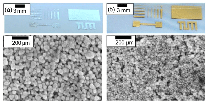
Figure 4Photos and SEM images of inkjet-printed films with the (a) silver nanoparticle ink DGP 40LT-15C, and (b) the gold nanoparticle ink Au-LT-20 (taken from Albrecht, 2018).
6.1 Conductor characteristics
After drying and sintering, the thickness of the gold nanoparticle conductive film is 193 nm and showed sheet resistance values down to 435 mΩ sq−1 on paper, which corresponds to 29 % of the conductivity of bulk gold. For the silver nanoparticle conductive film, the thickness is 700 nm and it showed sheet resistance of 55.4 mΩ sq−1, 42 % of the conductivity of bulk silver.
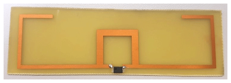
Both inks were printed on Paper and PET, resulting in four prototypes. Unfortunately, it was not possible to achieve a conductive layer on normal paper, so a non-biodegradable glossy-paper based substrate was used. Three layers of gold nanoparticle were printed for both substrates in order to reach a good conductivity, whereas for the silver ink, just one layer was sufficient. The RFID chip was attached after the antennas were sintered. Since soldering is not possible to connect the chip to the antenna due to the temperature range paper and PET can support, the chip was affixed with a conductive silver epoxy from Circuit Works. The gold NP ink printed tags are showed in Figs. 5 and 6.
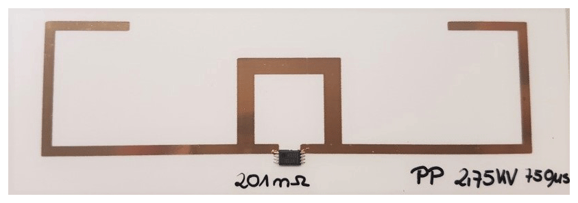
Figure 5Three layers gold nanoparticle film on paper based substrate connected to the chip by conductive silver epoxy.
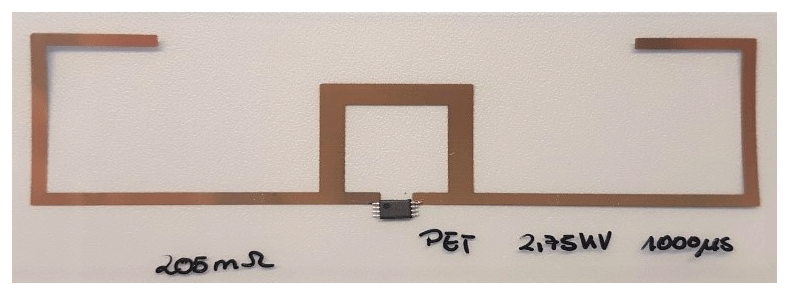
Figure 6Three layers gold nanoparticle film on PET substrate connected to the chip by conductive silver epoxy.
6.2 Read distance
The maximum distance at which a tag can be detected by the reader is an important practical tag performance indicator. Using the read range to evaluate the performance of RFID tags has also the advantage that it can be measured wirelessly, using rather unsophisticated equipment. This way, the problematic invasive small antenna measurements are avoided and separate characterization of the tag IC is not required.
The Impedance matching plays an important role in the tag performance. The better the impedance match, then the Power Transmission Coefficient τ tends to unity, which means a complete energy transmission as shown in the Eq. (3) (Rao et al., 2005).
where Rc and Ra are chip and antenna resistance, respectively. Zc and Za are chip and antenna impedance, respectively. Additionally, in Eq. (4) by making the use of the Friis free-space equation, the read range r between tag and antenna can be obtained:
where λ is the wavelength, Pr is the power transmitted by the reader, Gr is the reader antenna gain, Ga is the gain of the receiving tag antenna, and Pth is the minimum threshold power. The peak read range, r, across a frequency range can be referred to as the tag's resonance and will coincide with the maximum power transmission coefficient, τ.
6.2.1 Measurements
The read distance measurement was realized with the reader PUR-RMCU-500U from RF-Embedded and an UHF (865–868 MHz) Mid-Range antenna from Kathrein and are shown in the Table 1.
Table 1Read distance measurement of the reference etched tag and the four inkjet-printed tags.
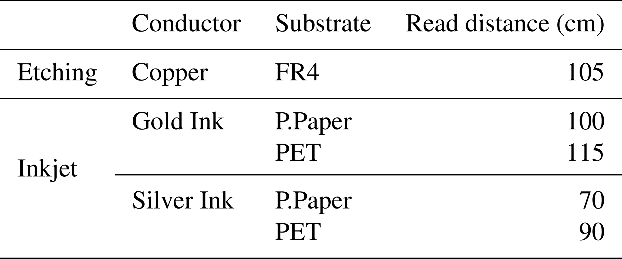
A very important factor to consider when performing the use of alternative materials in the development of tags is the reduction of the performance of the device, which happens in most cases, but depending on the application it is not an impediment in the implementation. But in contrast the tests showed that, compared to the prototype performed with etching technique, the gold ink on PET inkjet-printed tag, has a higher reading distance (a determining factor in the development of RFID tags). This could happen perhaps because of the accuracy of the measurement setup or also because of the variability of the chip impedance between two chips, it could cause a better matching with the gold ink.
6.2.2 S11 measurements
The S11 parameter is a very important indicator of the maximum power transfer of an antenna and it shows how much of the signal is being reflected in the transmission.
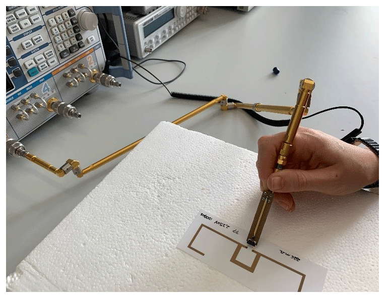
For all prototypes the antenna S11 parameter was simulated with CST Studio Suite and measured without the RFID chip with a ZVA40 vector network analyser from Rohde & Schwarz. The simulated design is shown in Fig. 7. A discrete port with the RFID chip impedance is used as feeding point for the simulation and the S-Parameter calculations. The simulations were realized with Time Domain solver and the boundary conditions are “open add space” in all directions. The measurement setup is shown in Fig. 8 as well as the connection between the RFID antenna and the vector network analyser (VNA) through a balance to unbalance converter (balun). The VNA including the measurement lines and the balun is calibrated with the OSM technique for one-port-calibration.
Figures 9 and 10 show the measurements for the gold NP inkjet-printed tags on paper based substrate and polymer based substrate, respectively. Figure 9 shows a worse outcome (red) in comparison with the simulated results (blue). On PET substrate, the measured results are more consistent with the simulations, especially regarding the resonant frequency.
The measurements for silver NP are shown in Fig. 11 on paper based substrate and Fig. 12 on polymer based substrate. The results were similarly to the gold NP results, worse for paper and better for PET substrate.
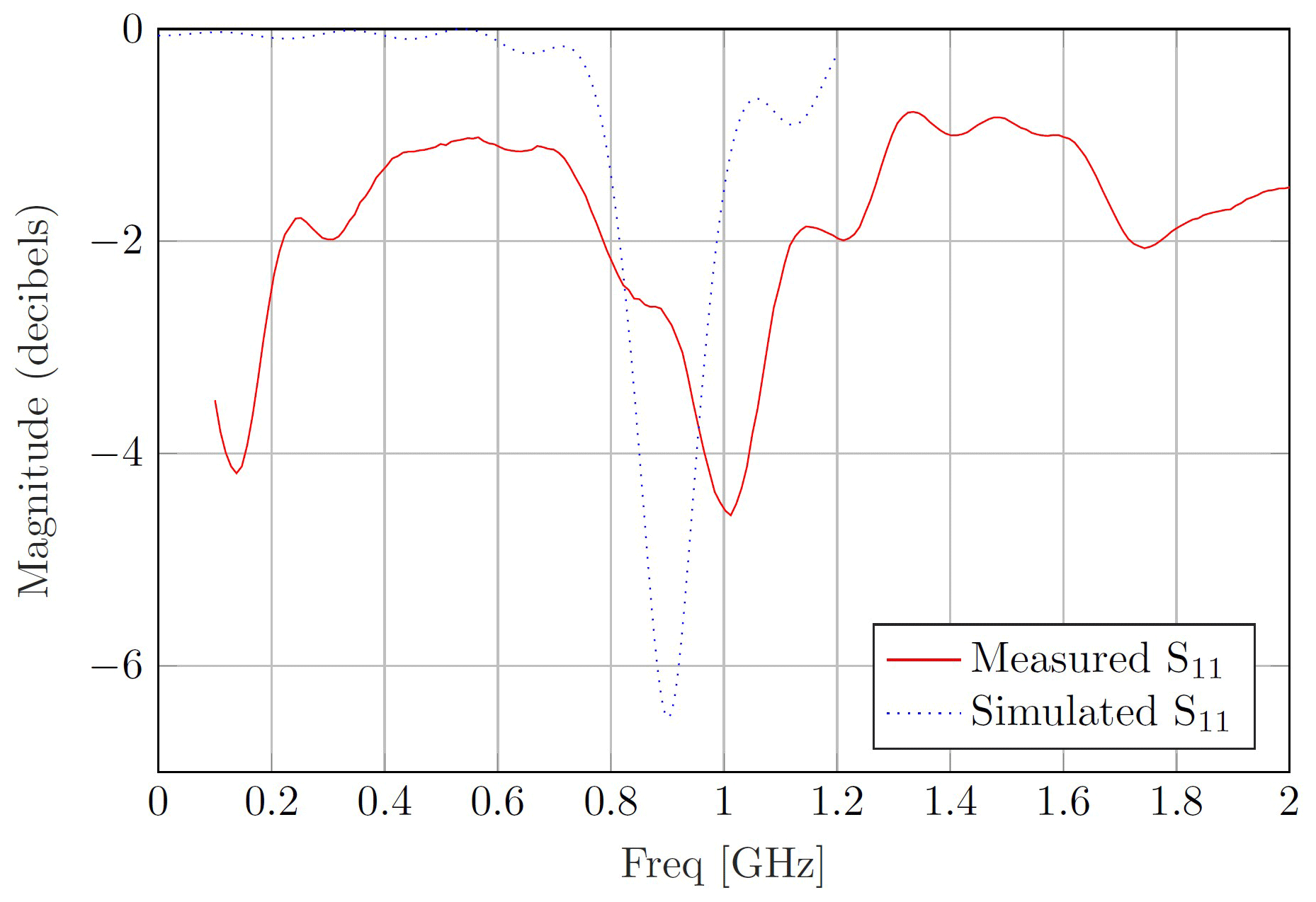
Figure 9S11 measured and simulated results of gold NP inkjet-printed tags on paper based substrate.

Figure 10S11 measured and simulated results of gold NP inkjet-printed tags on polymer based substrate.
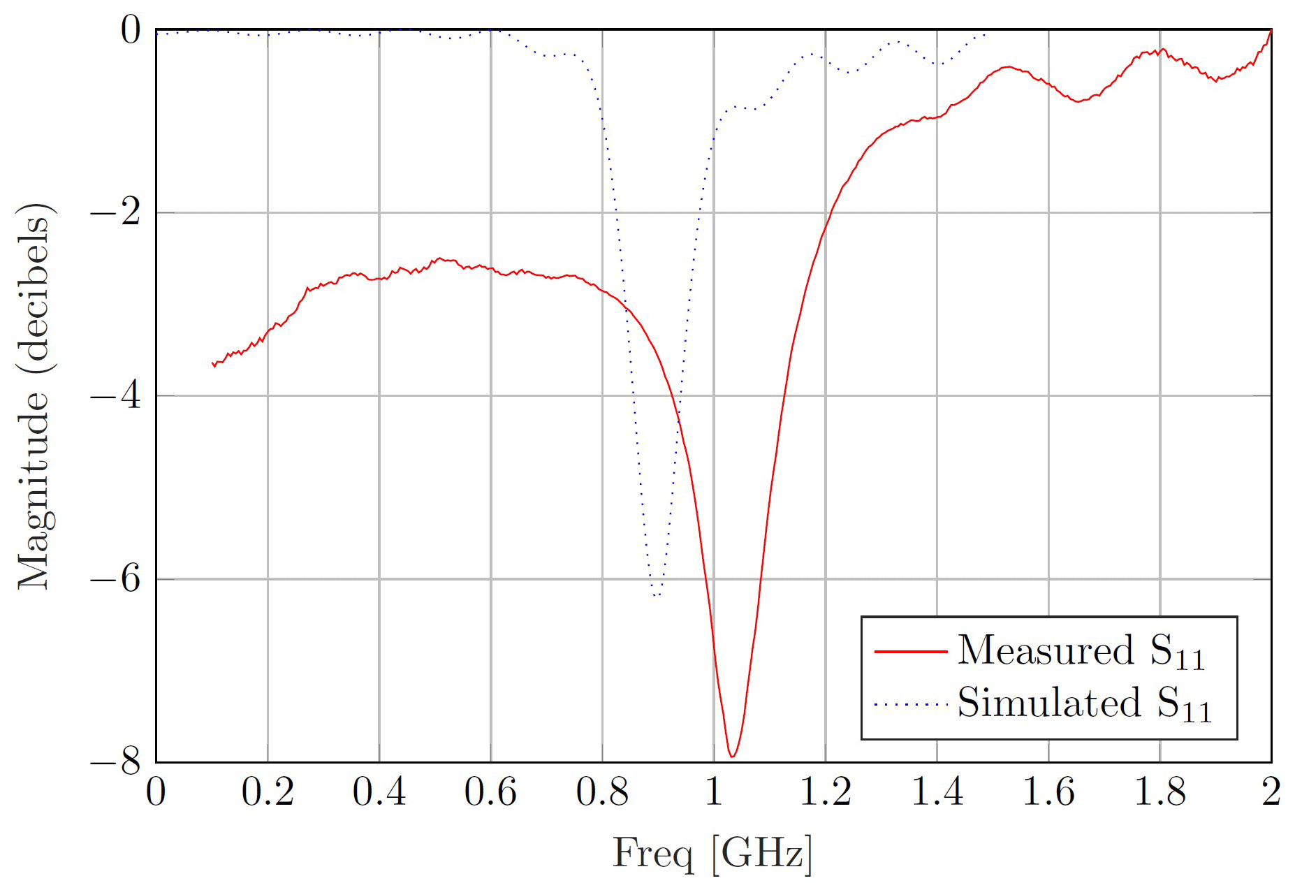
Figure 11S11 measured and simulated results of silver NP inkjet-printed tags on paper based substrate.
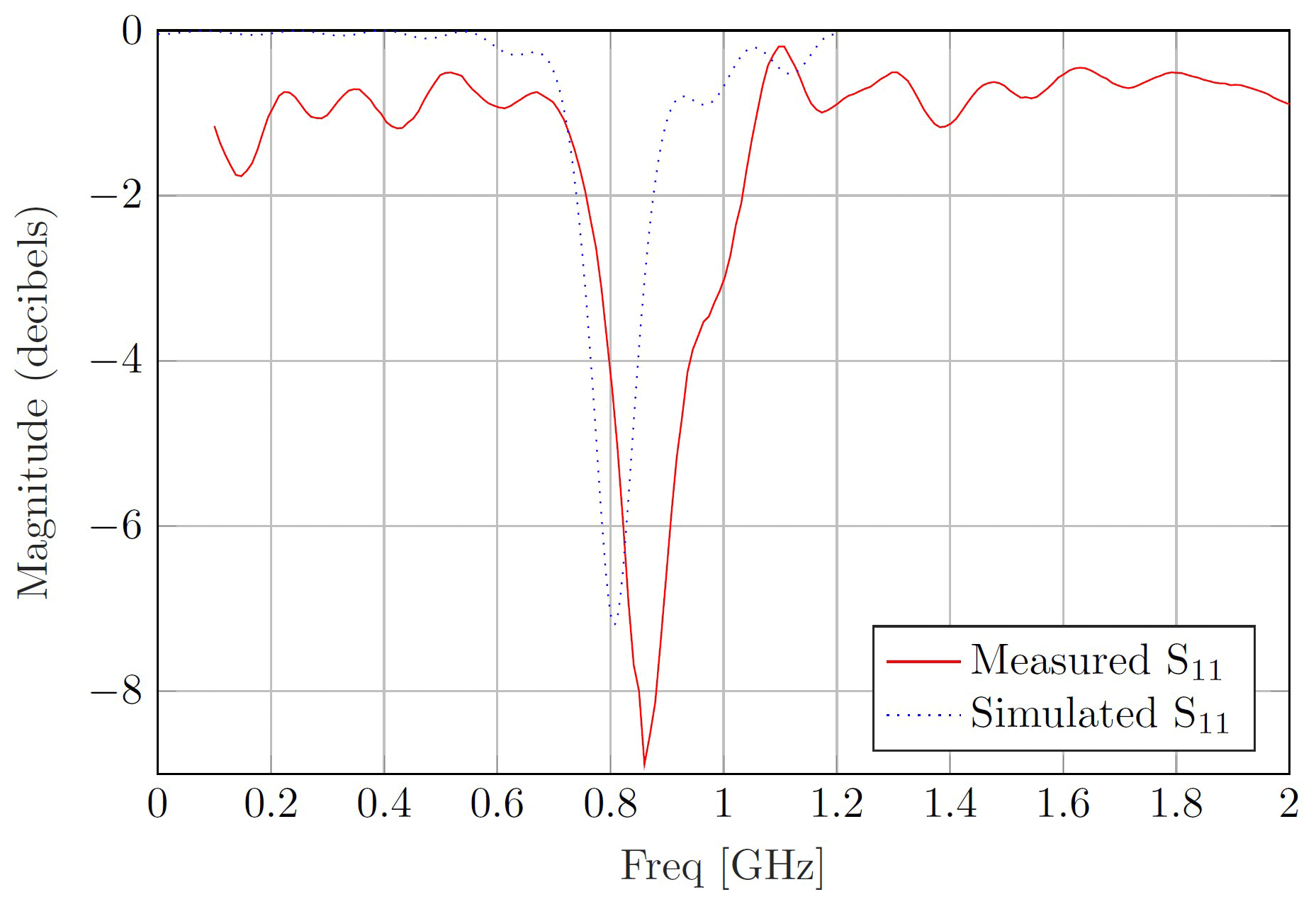
Figure 12S11 measured and simulated results of silver NP inkjet-printed tags on polymer based substrate.
For all the prototypes, the frequency shift is expected because of the change of the material without the design optimization. Moreover, the results from the vector network analyser measurements are referenced to 50 Ω and the incoherent insertion loss on the low frequencies were caused due to the balun used for the measurement which was not suitable for that frequency range. But the resonance frequency can be analysed anyway for the proof of concept.
When designing an antenna, the goal is to have maximum power transfer and a high antenna efficiency. The antenna design needs to be optimized for the right frequency with the specific conductors and substrates. From the same design shown in Fig. 1, for each tag and its materials, some adjustments in the length and thickness were realized to reach the better performance for the “greener”-tags.
Figures 13 and 14 show the simulated results for the new designs with the RFID chip attached before (blue) and after (orange) optimization for gold NP on the substrates photo paper and PET, respectively. As well as Figs. 15 and 16 show the simulated silver NP results for the new designs with the RFID chip attached before (blue) and after (orange) optimization on the substrates photo paper and PET, respectively.
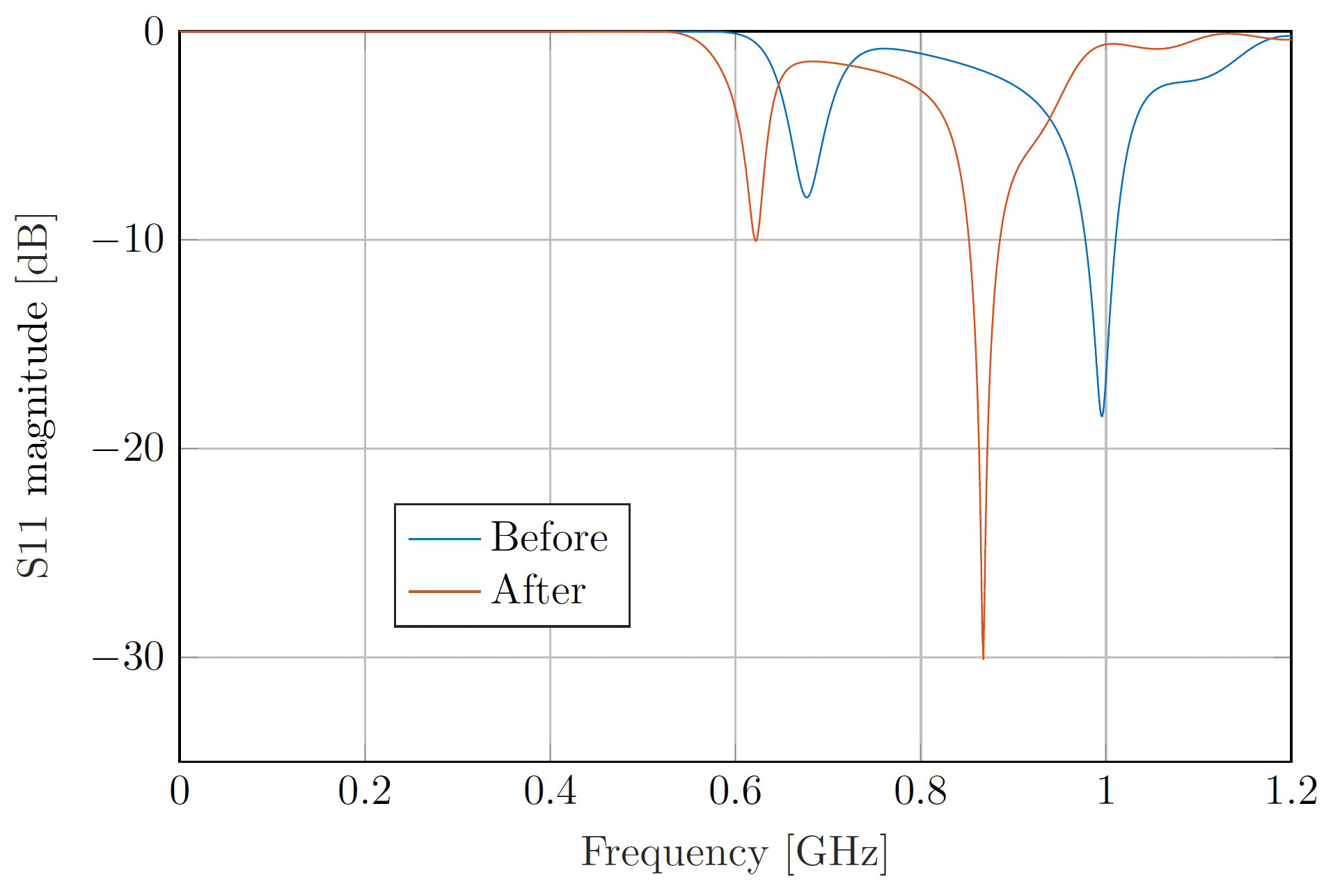
Figure 13Simulated S11 before and after design optimization for gold NP on paper based substrate.
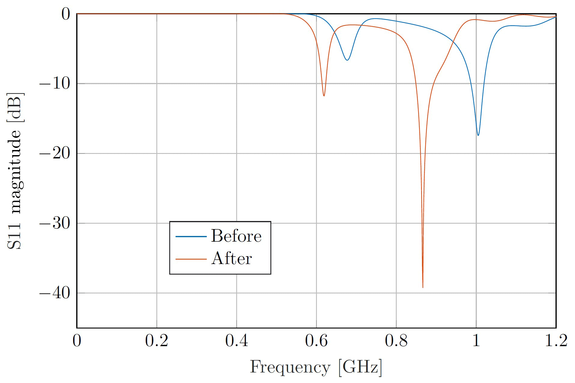
Figure 14Simulated S11 before and after design optimization for gold NP on polymer based substrate.
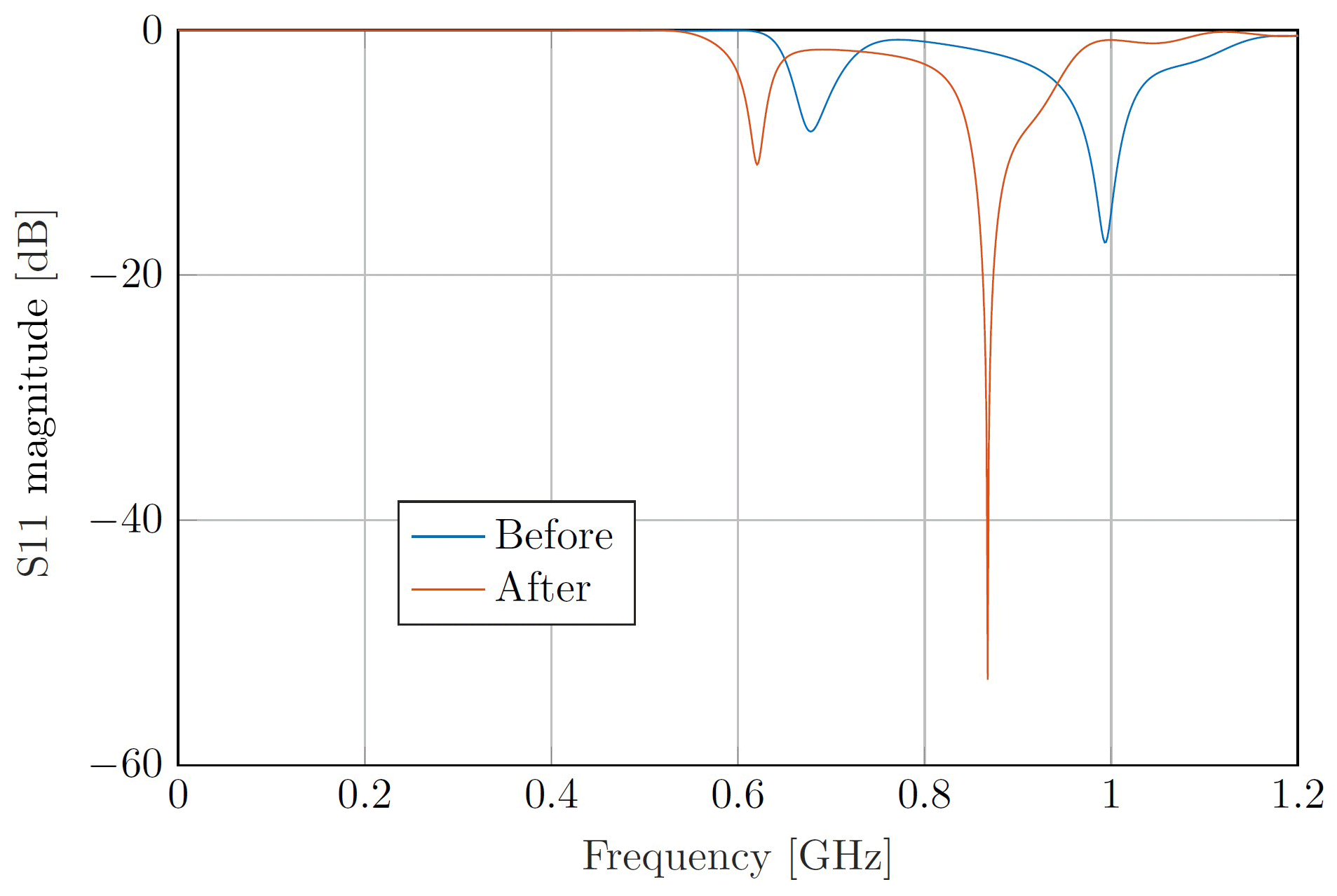
Figure 15Simulated S11 before and after design optimization for silver NP on paper based substrate.
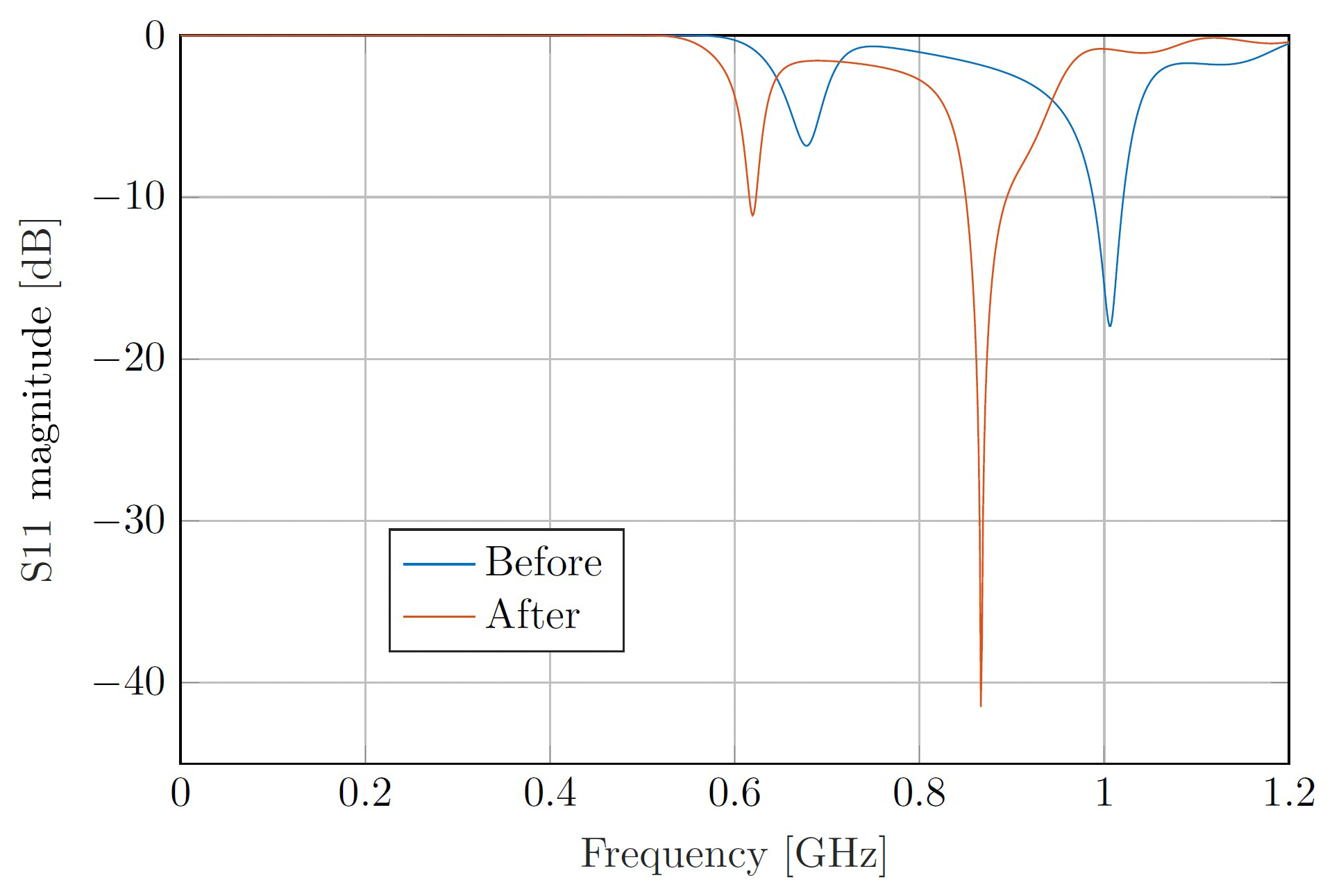
Figure 16Simulated S11 before and after design optimization for silver NP on polymer based substrate.
As one can see, the optimization is fundamentally necessary for a good performance of the RFID tag. At the UHF frequency 866 MHz, the simulated antennas show excellent return loss results as −30 and −39 dB for gold NP on paper and on PET substrate, respectively. For Silver NP the return loss is −53 and −41 dB on paper and PET substrates, respectively. The −10 dB bandwidth (BW) is around 40 MHz for all the tags.
In order to evaluate the performance of the antennas, Fig. 17 shows the simulated S11 parameters for the reference antenna design and the four proposed optimized antennas. The simulations show that all proposed antennas are well adjusted and at the exact resonance frequency. Some of the “greener” antennas present better S11 results than the reference antenna.
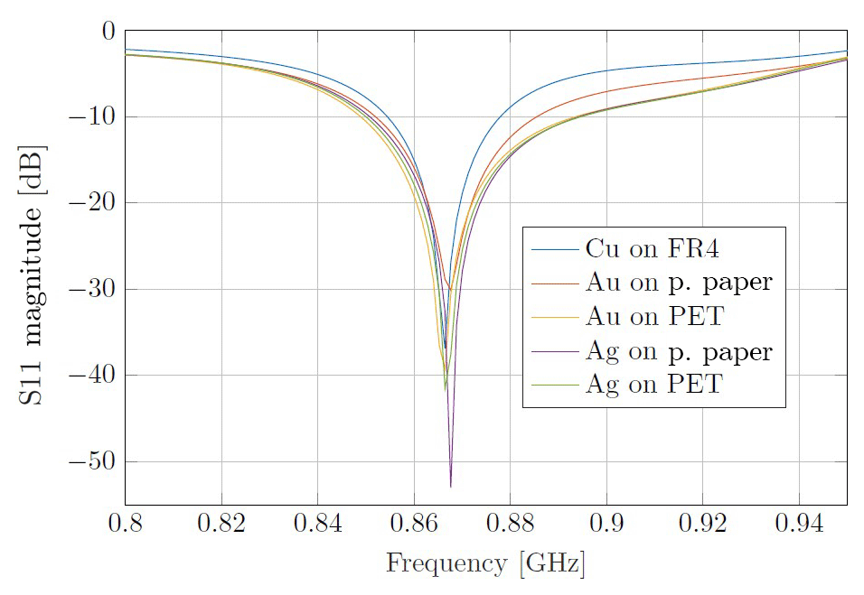
Figure 17Simulated S11 parameters for the reference antenna design of copper on FR4 substrate (blue), and the four proposed antennas gold on photo paper (orange), gold on PET (yellow), silver on photo paper (purple) and silver on PET (green).
For future work, the optimized designs should be manufactured and measured, to validate their increased performance.
This paper has shown the use of inkjet printing technique for gold and silver nanoparticles on organic and inorganic substrates in order to reduce the negative environmental impact of the traditional manufacturing techniques in RFID design. The use of a low cost consumer printer instead of a high resolution printer, makes the process even easier and faster without compromising the printing quality or RF performance.
In order to obtain a good conductivity, a IPL sintering on the inkjet-printed films was performed. This thermal curing procedure is able to reduce the resistance of the ink. The gold nanoparticles film, became conductivity solely after sintering.
Read distance measurements were conducted to evaluate the tag performance and even without correct antenna optimization, the gold nanoparticle tags showed similar or even better read range than the reference tag prototype performed with etching technique. The “greener” devices presented good performance and great RF results according to CST simulations.
This approach enables the manufacturing process in microwave circuit design to become more environmentally friendly and it results in many possibilities for application in bio-sensing, dissolvable electronics, flexible electronics, food sensors and implantable wireless devices.
All relevant models and results of the research are contained in the manuscript. The work can be reproduced with the presented models. The simulation models can be requested by the corresponding author.
BC conceptualized the core idea, performed the simulations. BC and AA performed the production of the samples. BC and PE performed the measurements. EW supervised the research and provided resources and feedback. BC prepared the manuscript with contributions from EB and PE.
The authors declare that they have no conflict of interest.
This article is part of the special issue “Kleinheubacher Berichte 2018”. It is a result of the Kleinheubacher Tagung 2018, Miltenberg, Germany, 24–26 September 2018.
This research has been supported by the Conselho Nacional de Desenvolvimento Científico e Tecnológico (grant no. 290013/2015-1).
This work was supported by the German Research Foundation (DFG) and the Technical University of Munich (TUM) in the framework of the Open Access Publishing Program.
This paper was edited by Jens Anders and reviewed by two anonymous referees.
Albrecht, A.: Printed Sensors for the internet of things, Technical University of Munich, 2018.
Albrecht, A., Rivadeneyra, A., Salmerón, J., Abdellah, A., and Lugli, P.: Inkjet Printing and Photonic Sintering of Silver and Copper Oxide Nanoparticles for Ultra-Low-Cost Conductive Patterns, J. Mater. Chem. C, 4, 3546–3554, https://doi.org/10.1039/C6TC00628K, 2016.
Arebey, M., Hannan, M., Basri, H., Begum, R., and Abdullah, H.: RFID and Integrated Technologies for Solid Waste Bin Monitoring System, Proceedings of the World Congress on Engineering Vol. I, Elsevier, London, 2010.
Cummins, G. and Desmulliez, M.: Inkjet printing of conductive materials: a review, Circuit World, 38, 193–213, https://doi.org/10.1108/03056121211280413, 2012.
Delen, D., Sharda, R., and Hardgrave, B.: The promise of RFID-based sensors in the perishables supply-chain, IEEE Wirel. Commun., 18, 82–87, https://doi.org/10.1109/MWC.2011.5751300, 2011.
Dobkin, D.: The RF in RFID, Newnes, Elsevier, USA, https://doi.org/10.1016/B978-0-7506-8209-1.X5001-3, 2008.
Duroc, Y. and Kaddour, D.: RFID potential impacts and future evolution for green projects, Elsevier, France, https://doi.org/10.1016/j.egypro.2012.05.021, 2012.
Finkenzeller, K.: RFID Handbook Fundamentals and Applications in Contactless Smart Cards, Radio Frequency Identification and Near-Field Communication, 3rd Edn., Wiley, UK, 2010.
Qing, X. and Yang, N.: A folded dipole antenna for RFID, IEEE AP-S, 1, 97–100, 2004.
Rao, K., Nikitin, P., and Lam, S.: Impedance Matching Concepts in RFID Transponder Design, Fourth IEEE Workshop on Automatic Identification Advanced Technologies, USA, https://doi.org/10.1109/APS.2004.1329562, 2005.
Wunscher, S., Abbel, R., Perelaer, J., and Schubert, U.: Progress of alternative sintering approaches of inkjet-printed metal inks and their application for manufacturing of flexible electronic devices, J. Mater. Chem. C, 2, 10232–10261, https://doi.org/10.1039/C4TC01820F, 2014.