 | 10 Dec 2020
Experimental Investigation of a Nonlinear Energy Storage Effect due to High Power Electromagnetic Excitation
Robert Michels
Martin Schaarschmidt
Frank Gronwald
The susceptibility of interference victims can significantly be influenced by the presence of nonlinear circuit elements. In addition to the well known occurrence of intermodulation-frequencies, other effects can be observed as well. Recently, a nonlinear energy storage effect has been discovered which is due to the presence of nonlinearly loaded loop antennas if excited by an HPEM-excitation. In this contribution, this effect is further studied by experiment. It is seen that the nonlinear energy storage effect can be reproduced by means of a rather simple experimental setup. This allows to straighforwardly study parameter variations in order to attain an improved understanding of the considered effect.
- Article
(5493 KB) - Full-text XML
- BibTeX
- EndNote


Nonlinear lumped elements can lead to complex and a priori surprising effects regarding electromagnetic compatibility, as has been pointed out by Kanda (1980), Krauthäuser et al. (2002) and Rambousky et al. (2014), for example. More recently, in Kalantarnia et al. (2020) a nonlinearly loaded microstrip line inside a perforated metallic enclosure was analyzed by splitting the whole nonlinear structure into a linear part and a nonlinear load in order to combine the benefits of time domain and frequency domain analysis. Along these lines, it was observed, first by simulation, that the rectifying property of a diode can lead to a DC component in the response of a nonlinearly loaded antenna which is subject to a pulsed HPEM-excitation (Kotzev et al., 2017). This DC component may remain after the usual oscillations caused by the pulsed excitation have completely decayed. It represents electric field energy which is stored in the vicinity of the nonlinearly loaded antenna. Further studies have revealed that this DC component can significantly be increased by repetitive pulses. This phenomenon has been studied on a numerical basis (Michels et al., 2019) and it has also been experimentally verified, using a rather complex experimental setup (Michels et al., 2020).
In the following, we utilize a more elementary experimental setup which already exhibits the aforementioned nonlinear energy storage effect. This setup allows to experimentally investigate the influence of certain parameters on the nonlinear effect, similar to the parametric numerical study presented in Michels et al. (2019), thus providing more insights into the nonlinear effect itself.
The paper is organized as follows: In Sect. 2, the test setup and the nonlinearly loaded antenna are introduced. In Sect. 3, the nonlinear effect is studied under the influence of repetitive excitations and other parameter variations. Theoretical interpretations of the measurement results are given in Sect. 4. Finally, Sect. 5 provides a short conclusion.
2.1 Test setup and antenna
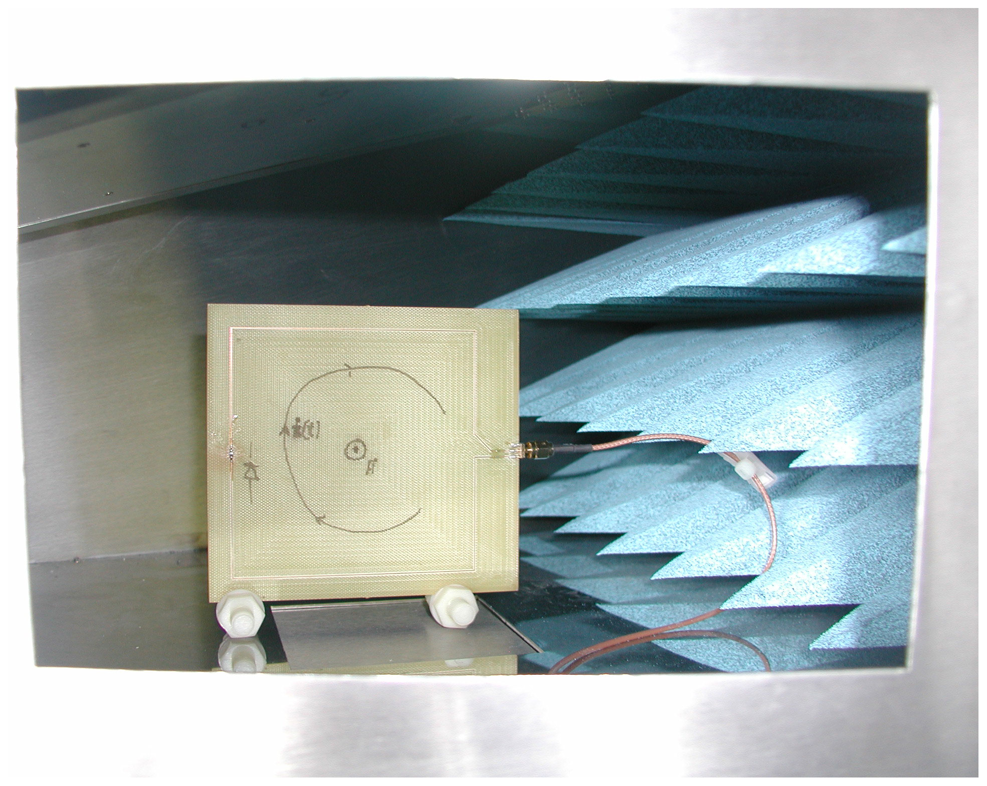
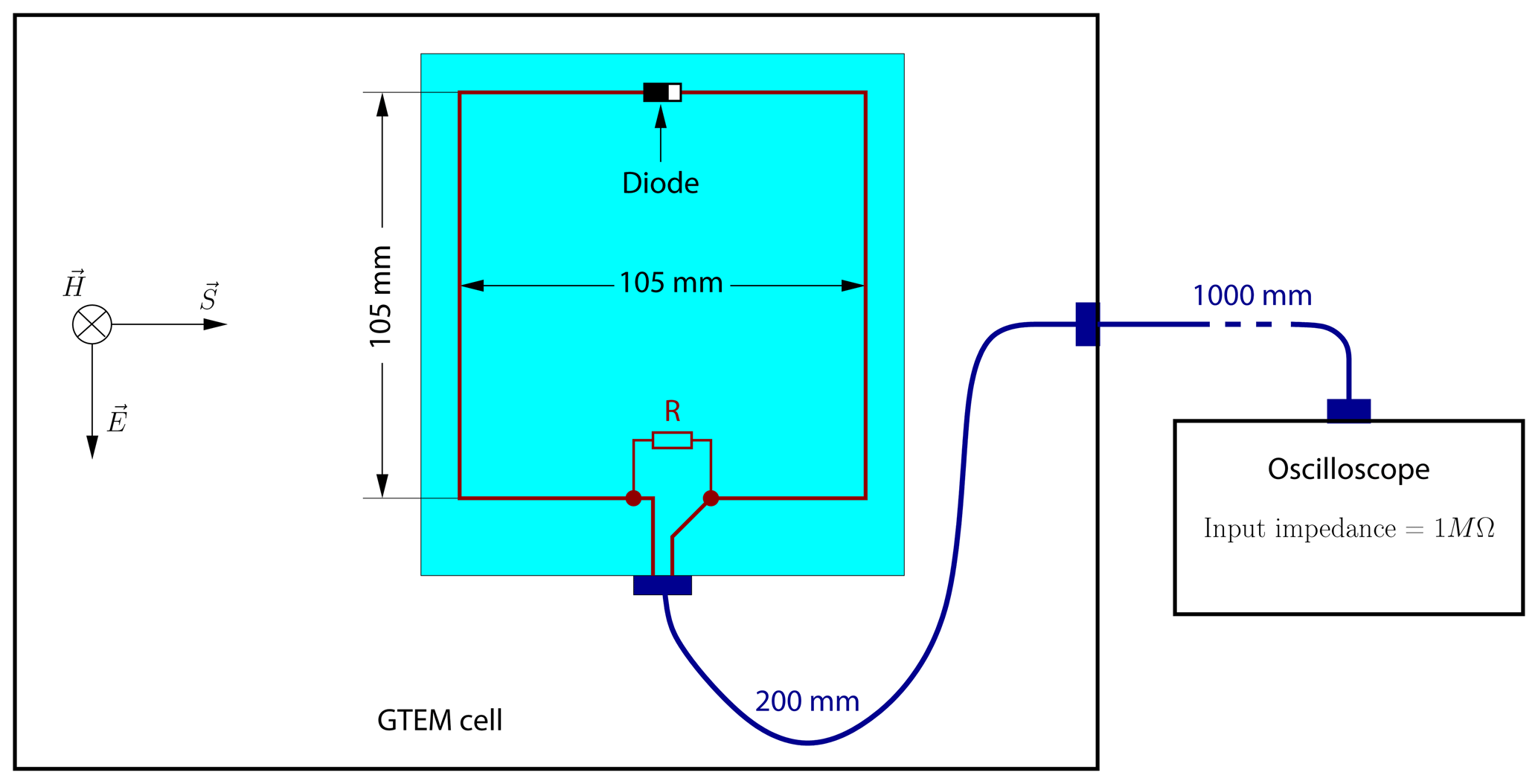
A nonlinearly loaded loop-antenna with dimensions as indicated in Fig. 1 and shown in Fig. 2 serves as device under test. The diode within the antenna is a Schottky-diode of type RB751. The nonlinearly loaded antenna is excited by one or several pulses inside a GTEM-cell (Schaffner GTEM 250). The pulses are generated by a corresponding pulse generator (AVTECH AVMH-4-C). The response of the antenna is recorded with an oscilloscope (Rhode & Schwarz, RTE 1024, 200 MHz). The input impedance of the oscilloscope is set to 1 MΩ to prevent a quick discharge of the diode.
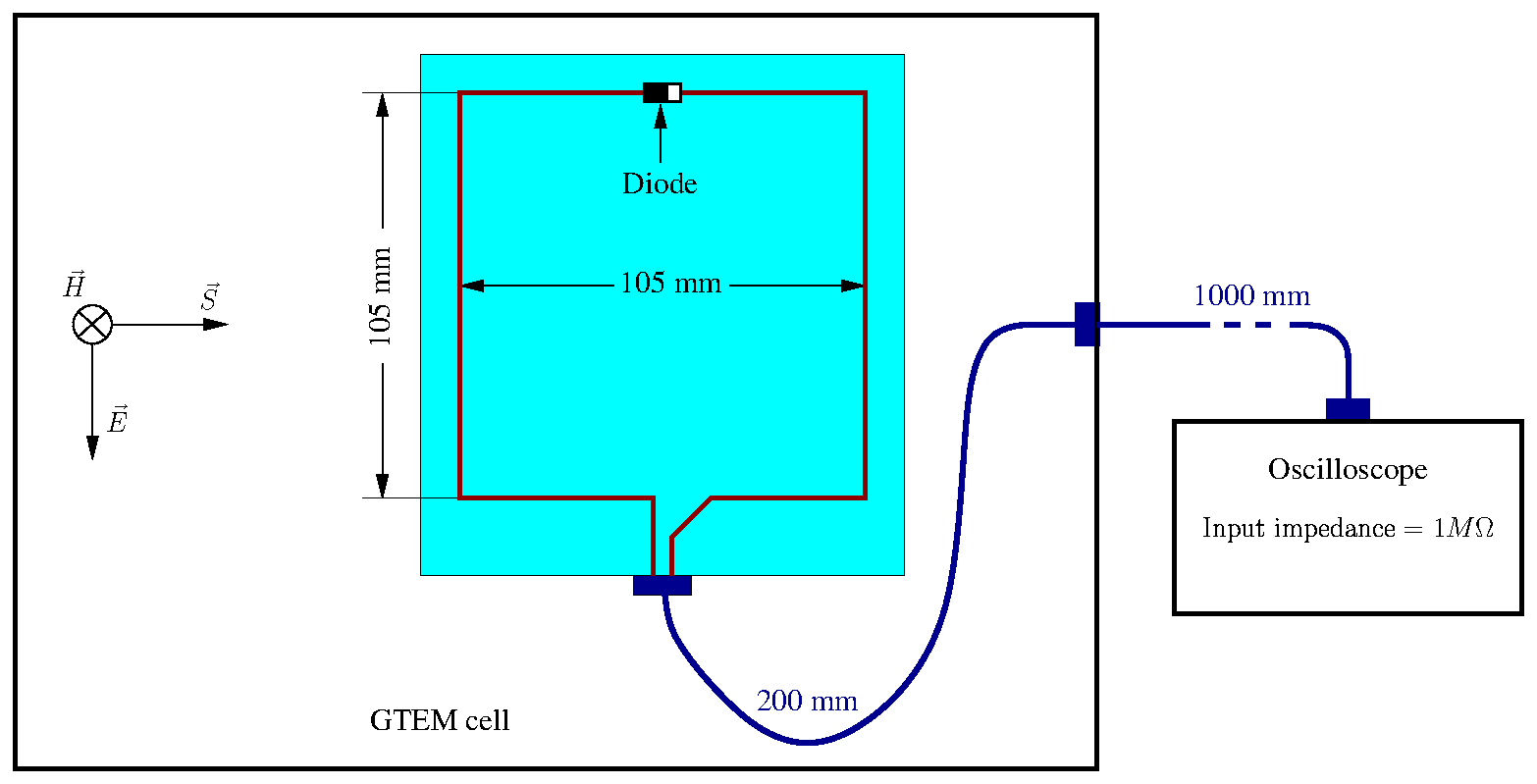
Figure 1Indicated test setup, showing the nonlinearly loaded antenna inside a GTEM-cell and subject to a field excitation.
2.2 Excitation pulse
An excitation signal V(t) is generated by the high-voltage pulse generator which approximately has the shape of a double exponential pulse. The signal at the output of the pulse-generator is measured via a 30 dB attenuator by the oscilloscope where the input impedance is set to 50 Ω. Then the output voltage of the pulse generator is given by
The measured excitation voltage is displayed in Fig. 3. It approximately follows the function
with the Heavyside-function Θ(t0) and the correction factor K(a,b),
together with the constants V0=37V, s−1, s−1, and t0=36.5 ns.
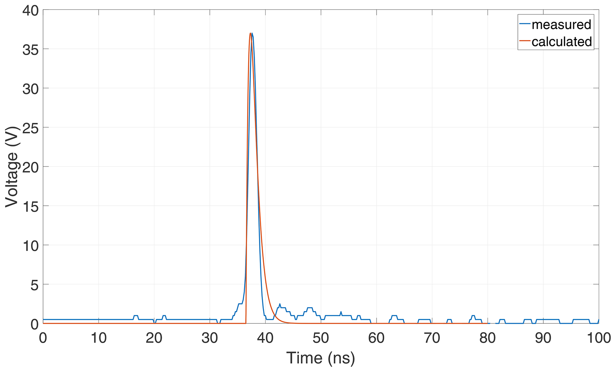
Figure 3Comparison between the measured voltage and the approximated double exponential pulse.
3.1 General antenna response in the linear and nonlinear case
To begin with, it is verified whether the nonlinear energy storage effect, which first was mentioned in Kotzev et al. (2017), can be reproduced by the given experimental setup. To this end, the receiving structure is first considered as linear, i.e., within the receiving antenna the diode is replaced by a wire bridge, compare Fig. 4.

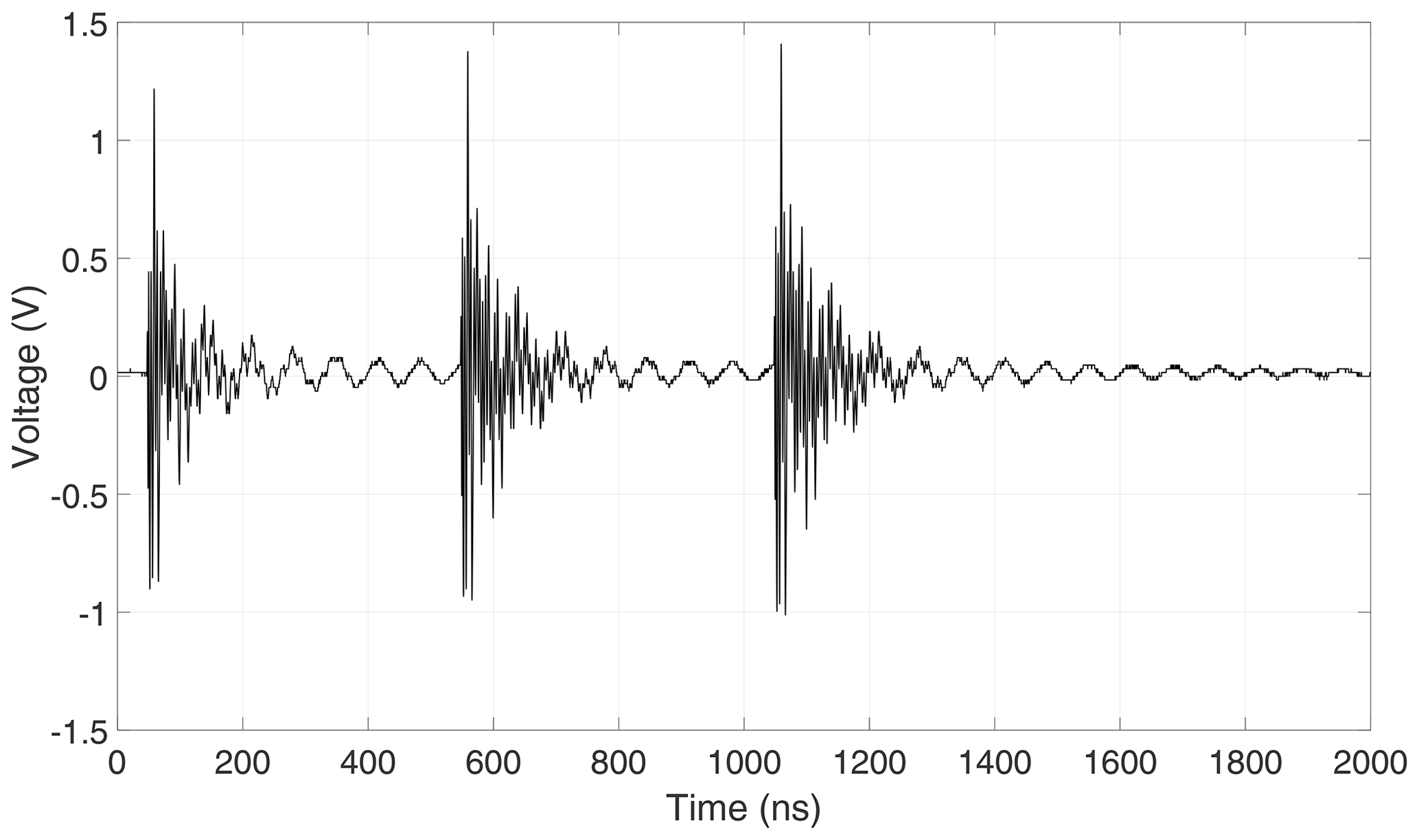
The linear antenna is excited by a train of three consecutive pulses at 500 ns intervals. The response shows decaying oscillations as a result of each pulse excitation, as can be seen in Fig. 5. In this case, there is no lasting DC component within the antenna response.
If the diode is inserted again, leading to the original configuration in Fig. 1, the response exhibits the behavior originally predicted by simulation for one pulse only (Kotzev et al., 2017), as shown in Fig. 6. A DC component remains after the completed decay of an oscillation caused by one pulse. Due to its long duration the DC component can be increased by repetitive pulses.
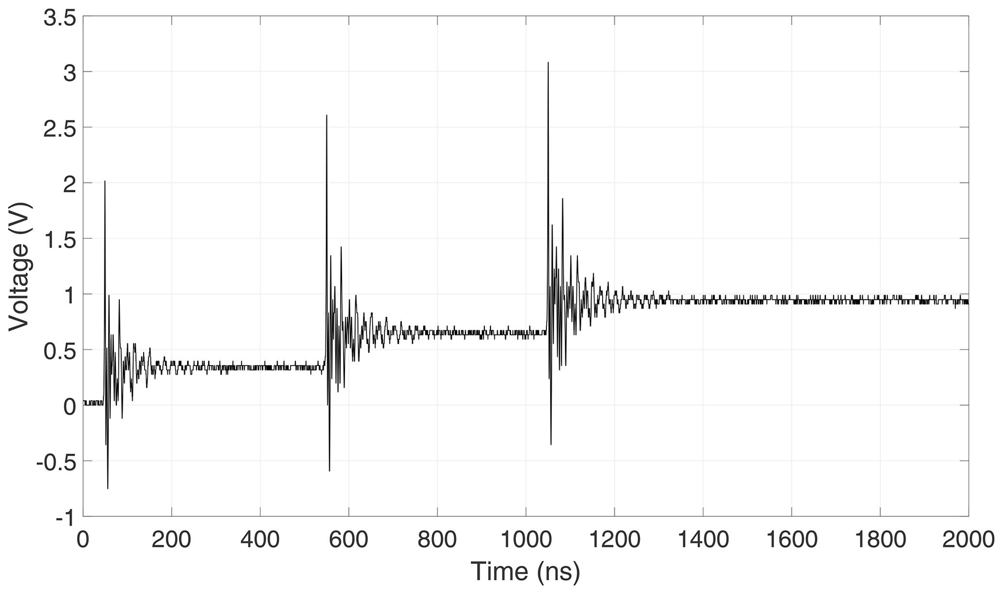
Figure 6Response of the nonlinearly loaded antenna at three consecutive pulses at 500 ns intervals.
It is therefore possible to amplify the energy storage effect if trains of pulses are applied under the condition that subsequent pulses occur before the complete decay of the DC component. This amplification has also be shown by simulations (Michels et al., 2019). In the following, some parameter modifications are performed in order to further study the nonlinear energy storage effect.
3.2 Variation of the excitation signal
For this subsection, excitation pulses with different peak-values were used, as shown in Fig. 7. As a result, the response of the nonlinearly loaded loop antenna shows higher peak values as well, leading to a faster increase of the DC component, as seen in Fig. 8. Numerically this somewhat obvious result has also been observed in Michels et al. (2019).
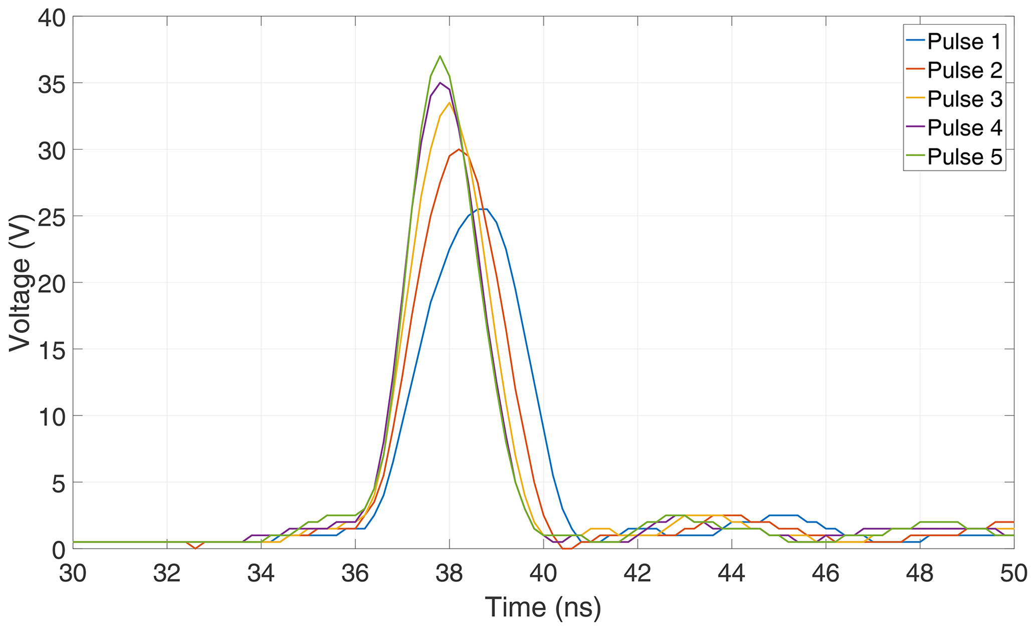

Figure 8Response of the nonlinearly loaded antenna at three consecutive pulses at 500 ns intervals with different peak values.
3.3 Reduction of the terminating resistance
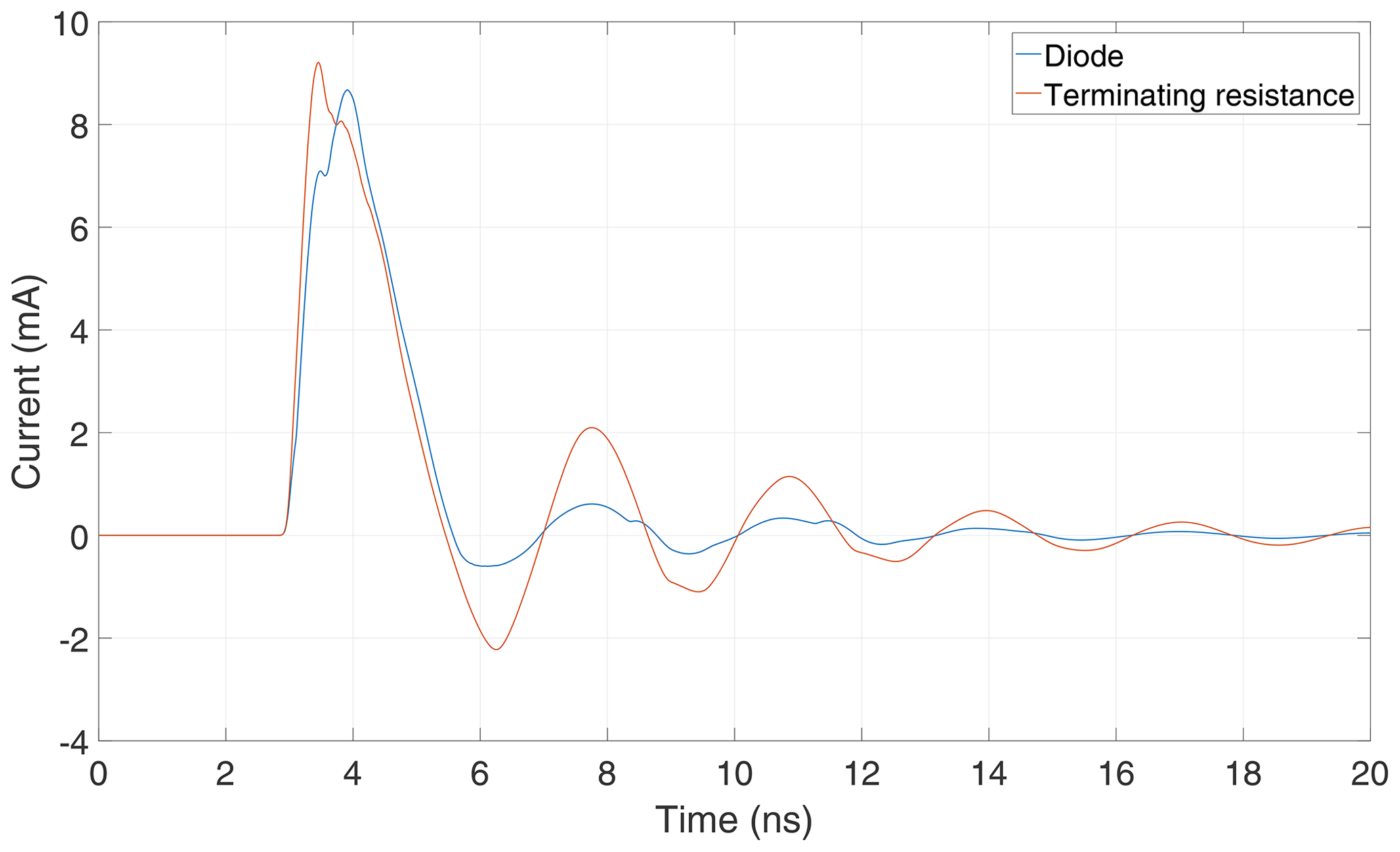
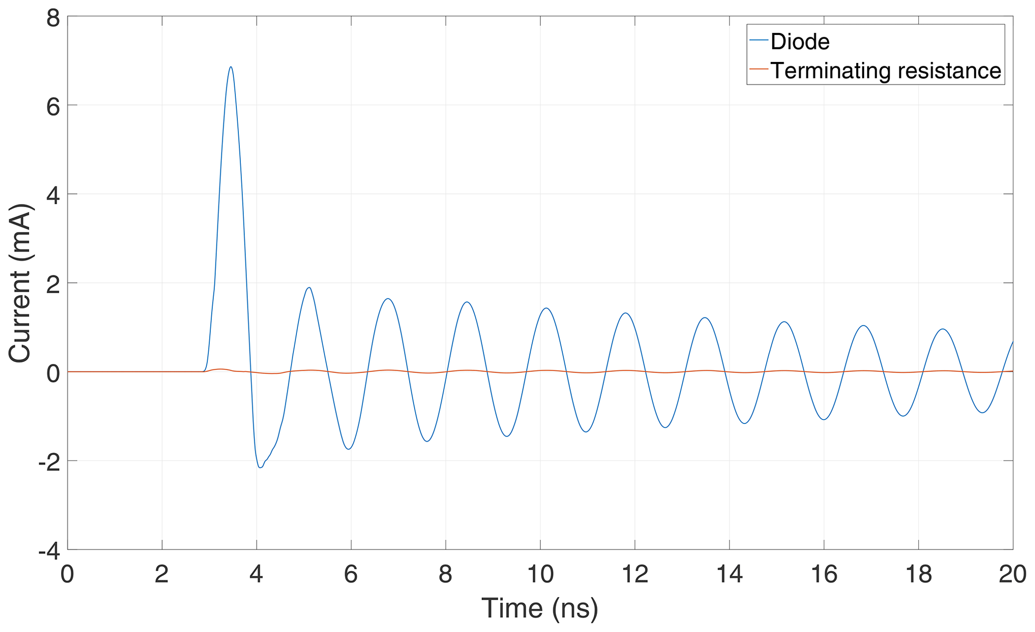
It is intuitively clear that lower resistances at the antenna port lead to a faster discharge of the stored energy. This is the reason why the energy-storage effect does not occur if the input impedance of the oscilloscope is matched to the impedance of the cable, i.e., matched to 50 Ω. A reduction of resistance is achieved by placing an additional resistor in parallel to the antenna port, as shown in Fig. 9.
The corresponding measurements show that the resulting DC component becomes smaller after each pulse if an additional terminating resistance is involved. Nevertheless, in Fig. 10 no remarkable change concerning the decrease of the DC component is observed as well. In fact, the DC component seems to be quite constant during the period inbetween two consecutive pulses. An explanation will be given in Sect. 4.
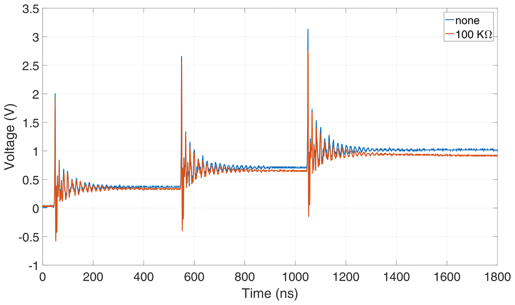
Figure 10Response of the nonlinearly loaded antenna to three consecutive pulses, with and without additional terminating resistance.
3.4 Increasing the parasitic capacitance of the diode
Another parameter variation consists in increasing the parasitic capacitance of the diode. To achieve this, an additional capacitor is put in parallel to the diode, as displayed in Fig. 11.

Figure 11Nonlinearly loaded loop-antenna with an additional capacitor parallel to the diode.
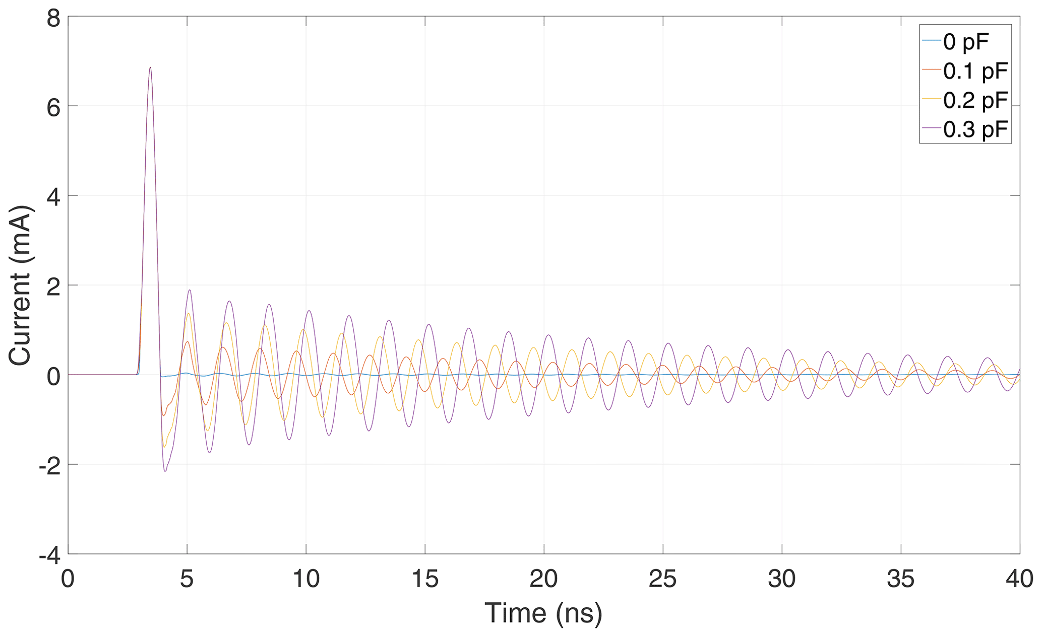
The measured response of the antenna shows, that higher parasitic capacitances decrease the DC component, compare Fig. 12. This result has also been observed in simulations (Michels et al., 2019).
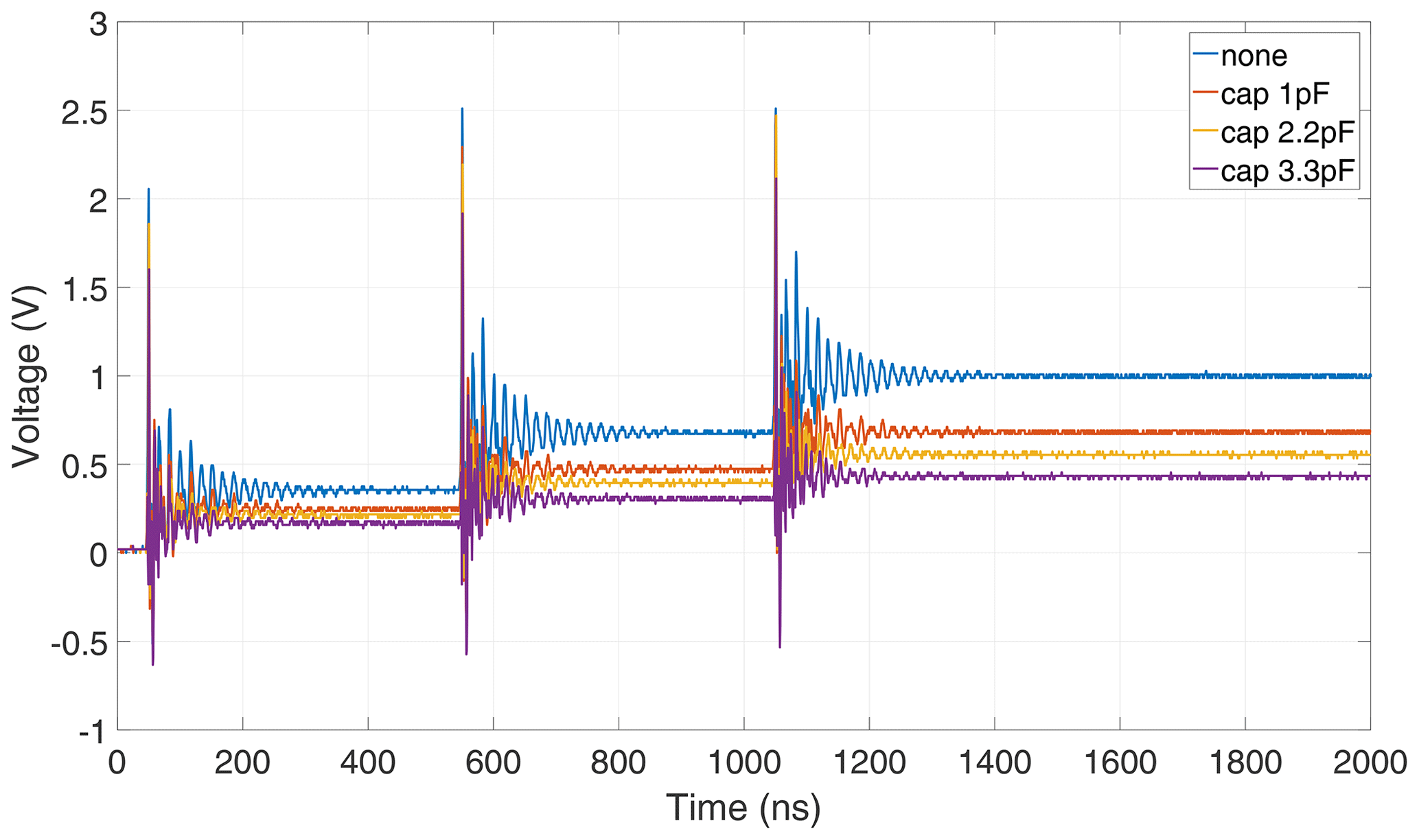
Figure 12Response of the nonlinearly loaded loop antenna to three consecutive pulses with additional capacitors parallel to the diode.
3.5 Changing the direction of incidence of the excitation
Another interesting parameter that can be varied is the direction of incidence of the excitation. From the induction law it can be concluded that the highest coupling to the antenna is achieved if the magnetic field component is directed perpendicular to the area spanned by the loop antenna. If the loop antenna is nonlinearly loaded with a diode its symmetry is broken. It is then of interest to study the effect of different orientations between the exciting field and the receiving antenna. Accordingly, two different mutual orientations are considered, as shown in Fig. 13.
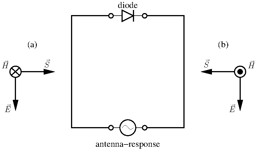
Figure 13Nonlinearly loaded loop-antenna and field excitation, given with two different orientations (a) and (b).
Clearly, for the case of a linear loop antenna both directions would lead to the same response. However, if the antenna is loaded with a diode, it turns out that the direction of incidence has an influence on the antenna response, as seen from Fig. 14. That is, in case of the direction designated by (a) the resulting DC component turns out to be higher if compared to direction (b). A comparison between the first and the third pulse shows that the difference between the two DC components is increased by each additional pulse.

In order to get a better understanding of the results observed by measurement, it is useful to perform full wave simulations. These allow to obtain qualitative values that are difficult to derive from measurements. For example, one value of interest is the current through the diode. All following simulations are performed with a time domain solver (CST, 2018).
4.1 Simulation set-up
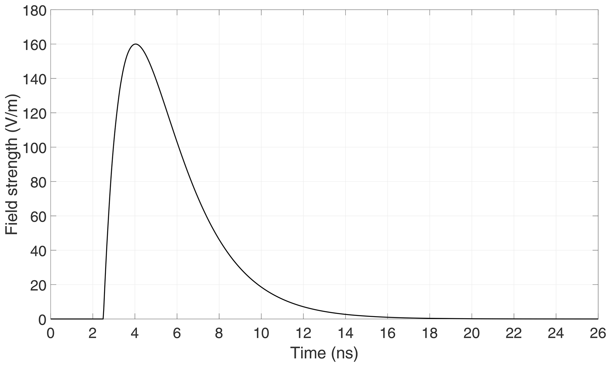
The nonlinearly loaded loop antenna is modeled within the full wave simulation software and excited by a plane wave, as sketched in Fig. 15. The plane wave carries a double-exponential pulse, analogous to the one introduced in Sect. 2.2 with the voltage V0 replaced by a field strength E0. Its explicit form is displayed in Fig. 16 and calculated from Eqs. (2), (3) with values , s−1, s−1, and t0=2.5 ns.
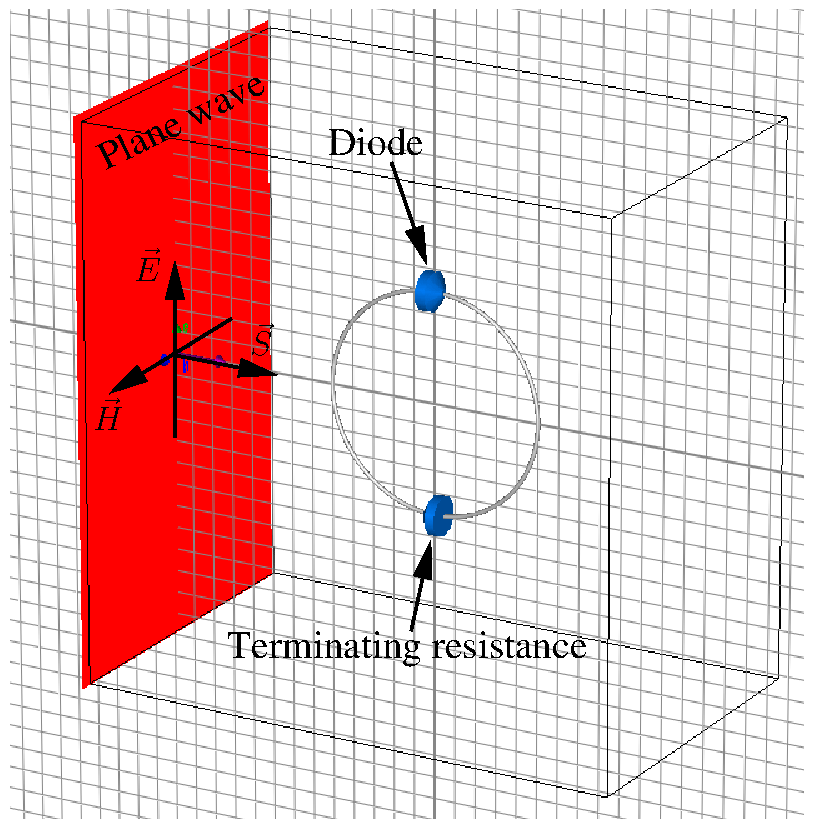
Figure 15Nonlinearly loaded loop-antenna excited by a plane wave within the simulation software.
4.2 Interpretation of measurement results obtained from variations of the terminating resistance and the parasitic capacitance
The currents through the diode and the terminating resistance are derived from simulation. First, the parasitic capacitance of the diode is set to 0.3 pF while the terminating resistance is varied in the following simulations.
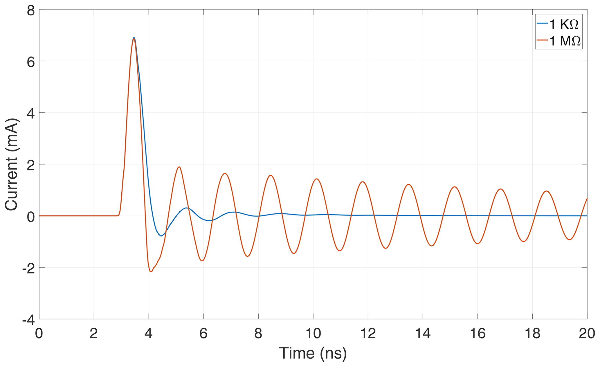
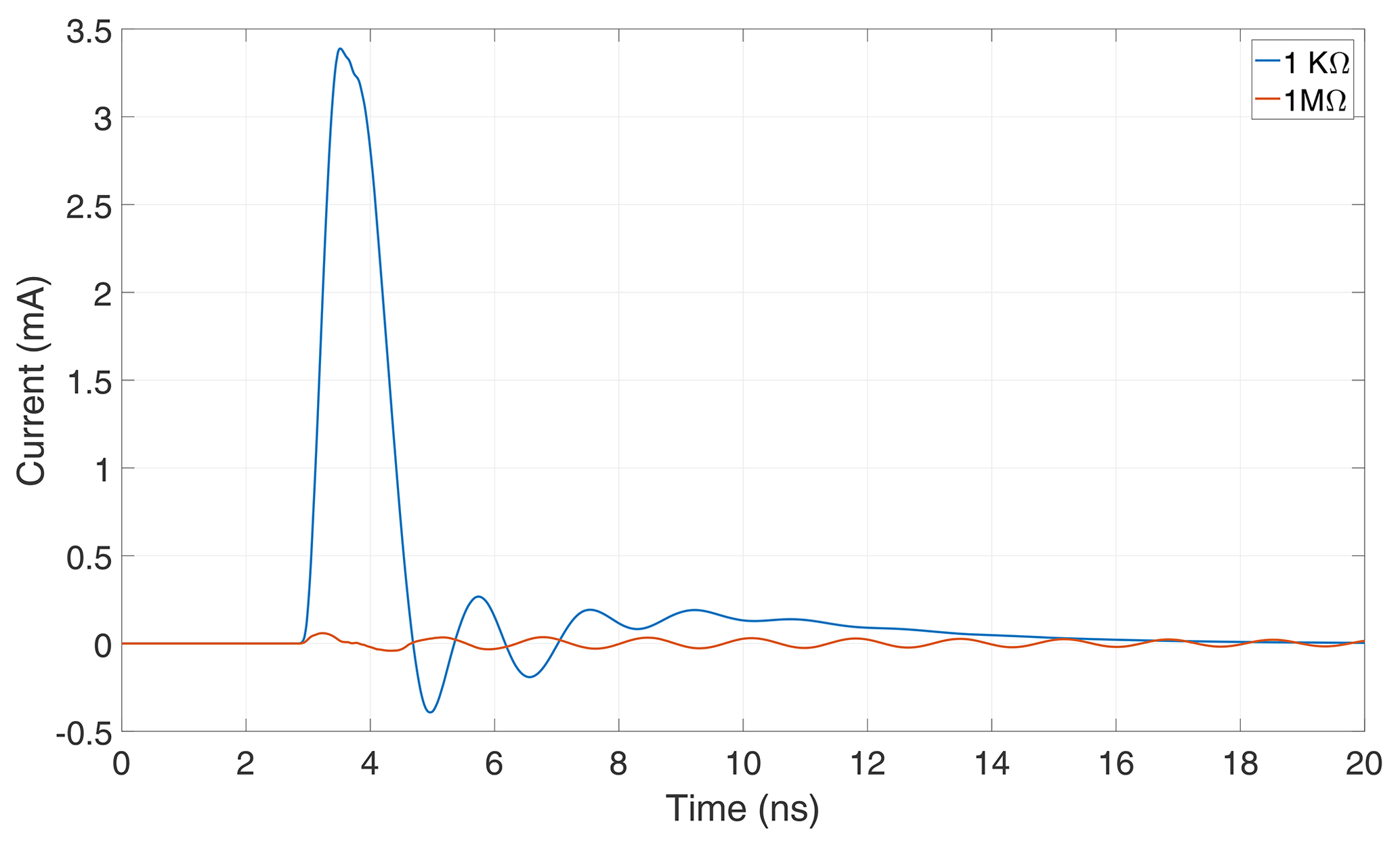
The first oscillation in Fig. 17 shows that the arithmetic mean of the current through the diode deviates significantly from zero. In addition, it only slightly depends on the terminating resistance. These currents are compared to the current flow through the terminating resistance presented in Fig. 18. Contrary to the diode current, the arithmetic mean of this current depends on the terminating resistance.
In order to show how a DC component can occur, the case of a 50 Ω terminating-resistance is considered first. The arithmetic mean of the current-flow through the diode is similar to the one of the current-flow through the terminating resistance, see Fig. 19. This implies a discharge via the terminating resistance. As a result, no DC component can emerge in the antenna-response, compare the discussion of Sect. 3.3.
In Fig. 20 the same constellation with a terminating-resistance of 1 MΩ is considered. In this case, the charge caused by the rectifying effect of the diode is only partially unloaded by the terminating resistance. If this resistance is sufficiently small, a significant discharge occurs. For higher resistances a certain amount of charge remains stored. The discharge becomes smaller with higher terminating resistances, compare Fig. 18. The stored charge is responsible for the emergence of a DC component in the antenna-response. This explains how the increase of the terminating resistance enhances the observed energy storage effect.
Next the parasitic capacitance of the diode, which so far was set to 0.3 pF, is varied. From the simulation results of Fig. 21 it can be seen that the DC part of the diode current is independent from the value of the parasitic capacitance. The charge has to be distributed between the antenna capacitance and the parasitic capacitance of the diode. If the parasitic capacitance of the diode is increased, the same charge is stored in a higher capacitance which leads to a lower voltage on the terminating resistance. This explains the results of the measurements performed in Sect. 3.4.
4.3 Interpretation of measurement results obtained from different directions of incidence
In Sect. 3.5, experiments were performed with two different directions of incidence. These revealed that the direction of the excitation has an influence on the behavior of the nonlinearly loaded receiving structure, as seen from Fig. 14. In order to examine this effect, the response to the first pulse is considered in more detail.
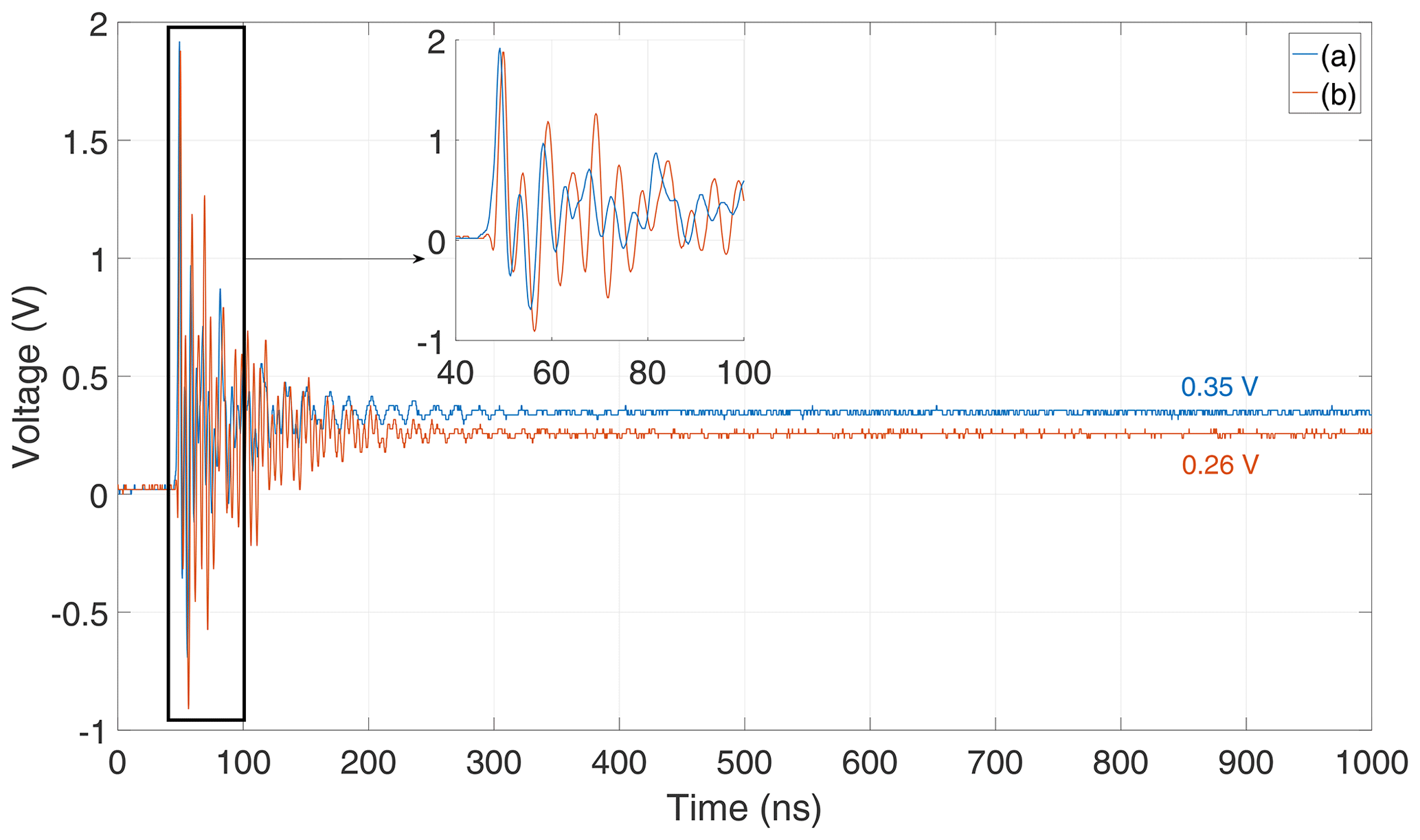
Figure 22Response of the nonlinearly loaded loop-antenna excited from two different directions of incidence.
The response is shown in Fig. 22 and reveals that the DC component in constellation (a), compare Fig. 13, is higher than the one in constellation (b). Considering the first oscillation it is seen that the signal of constellation (b) is delayed compared to constellation (a).
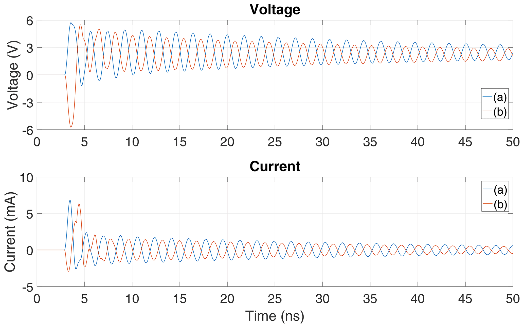
Figure 23Simulation results with voltage on the antenna port and the current through the diode when the antenna is excited with a field from two different directions of incidence.
In this case it is also helpful to study the current through the diode and the voltage at the antenna port. For that purpose, simulations analogous to the ones presented in Sect. 4.1 with the two directions of incidence are performed. The results of these simulations are displayed in Fig. 23. It is seen from the current through the diode that in constellation (a) the first half-wave contributes to the DC-term. The DC-term of constellation (b) is provided by the second half-wave. In summary we can state that if the direction of incidence of the electromagnetic wave that is carrying the transient pulse excitation is chosen according to (a), the diode is polarized in forward direction during the first half-wave and the charging process takes place. However, if the excitation is directed according to (b), the diode is polarized in reverse direction during the first half-wave. In that case the charging process takes place not until the second half-wave occurs. Due to ohmic and radiation losses, the second half-wave of the current has a smaller peak-value if compared to the first. Hence, less charge accumulates in the antenna and its parasitic capacitances which leads to a smaller DC component of the voltage at the terminating resistance of the antenna.
It has experimentally been observed that the nonlinear energy storage effect, that was first mentioned in Kotzev et al. (2017), can be amplified if repetitive pulses are applied as excitation. In view of parameter variations it was demonstrated that an increase of the excitation pulses peak leads to a higher DC component in the voltage response of the nonlinearly loaded loop-antenna, as also is clear from intuition. The DC component also depends on the terminating resistance at the antenna port. A reduction of this resistance leads to a smaller DC component. Furthermore, it was shown and explained that a higher parasitic capacitance of the nonlinear load can weaken the observed effect. Finally, it turns out that also the direction of incidence of the exciting plane wave has an influence on the DC component in the antenna response. These experimental observations also correlate with the predictions made by simulation in Michels et al. (2019).
The data presented in this article are available from the authors upon request.
The measurements, computer simulations, and data processing including all graphical representations were carried out by RM. Editorial hints as well as mathematical and physical suggestions were given by MS and FG.
The authors declare that they have no conflict of interest.
This article is part of the special issue “Kleinheubacher Berichte 2019”. It is a result of the Kleinheubacher Berichte 2019, Miltenberg, Germany, 23–25 September 2019.
This research has been supported by the Bundeswehr Research Institute for Protective Technologies and CBRN Protection (WIS) (grant no. E/E590/JZ001/HF063).
This paper was edited by Lars Ole Fichte and reviewed by two anonymous referees.
CST: CST Microwave Suite 2018, available at: https://www.cst.com (last access: 9 September 2020), 2018. a
Kalantarnia, A., Keshtkar, A., and Ghorbani, A.: Predicting the Effects of HPEM Radiation on a Transmission Line Terminated With Linear/Nonlinear Load in Perforated Metallic Enclosure Using FDDM/VF, IEEE T. Plasma Sci., 48, 669–675, https://doi.org/10.1109/TPS.2020.2968759, 2020. a
Kanda, M.: Analytical and Numerical Techniques for Analyzing an Electrically Short Dipole with a Nonlinear Load, IEEE T. Antenn. Propag., 28, 71–78, https://doi.org/10.1109/TAP.1980.1142269, 1980. a
Kotzev, M., Bi, X., Kreitlow, M., and Gronwald, F.: Equivalent circuit simulation of HPEM-induced transient responses at nonlinear loads, Adv. Radio Sci., 15, 175–180, https://doi.org/10.5194/ars-15-175-2017, 2017. a, b, c, d
Krauthäuser, H. G., Tkachenko, S., and Nitsch, J.: The Action of Non-Linear Effects in a Resonator, Proc. of the XXXVIIth General Assembly of the International Union of Radio Science, URSI GA 2002, Maastricht, the Netherlands, 2002. a
Michels, R., Willenbockel, M., and Gronwald, F.: A Parametric Study of an Energy Storage Effect due to Nonlinear Components and HPEM-Excitation, 2019 International Symposium on Electromagnetic Compatibility – EMC EUROPE, September 2019, Barcelona, Spain, https://doi.org/10.1109/EMCEurope.2019.8871855, 2019. a, b, c, d, e, f
Michels, R., Kreitlow, M., Bausen, A., Dietrich, C., and Gronwald, F.: Modeling and Verification of a Parasitic Nonlinear Energy Storage Effect Due to High-Power Electromagnetic Excitation, IEEE T. Electromagn. C., https://doi.org/10.1109/TEMC.2020.2980976, online first, 2020. a
Rambousky, R., Tkachenko, S., and Nitsch, J.: A novel solution algorithm for nonlinearly loaded transmission lines inside resonating enclosures, Adv. Radio Sci., 12, 135–142, https://doi.org/10.5194/ars-12-135-2014, 2014. a