 | 17 Dec 2021
A 10 kHz to 6 GHz Low-Cost Vector Network Analyzer
Andreas Depold
Stefan Erhardt
Robert Weigel
Fabian Lurz
This publication introduces a low-cost vector network analyzer with very large frequency range made of commercial off-the-shelf components. It utilizes two identical receivers and two directional bridges to allow for two fully bidirectional measurement ports. The design surpasses the performance of competing low-cost network analyzers in regards of dynamic range, frequency span and calibration capability.
- Article
(5528 KB) - Full-text XML
- BibTeX
- EndNote


Vector network analyzers (VNAs) are fundamental tools for engineers working with radio frequencies (RF). High end devices come with a high price which causes them to be out of reach for most small companies and amateur radio enthusiasts. While affordable devices exist, most currently available very low-cost VNAs are of transmission/reflection () type with fairly limited performance. With that kind of architecture only two of the four two-port scattering parameters can be measured, which, while enough in many cases, limits the way the device can be calibrated and therefore reduces measurement accuracy.
This paper presents a relatively low-cost device made out of commercial off-the-shelf components that outperforms competing low-cost alternatives. First an overview over the design is given, followed by implementation details. Some example measurements and the achieved specifications are shown.
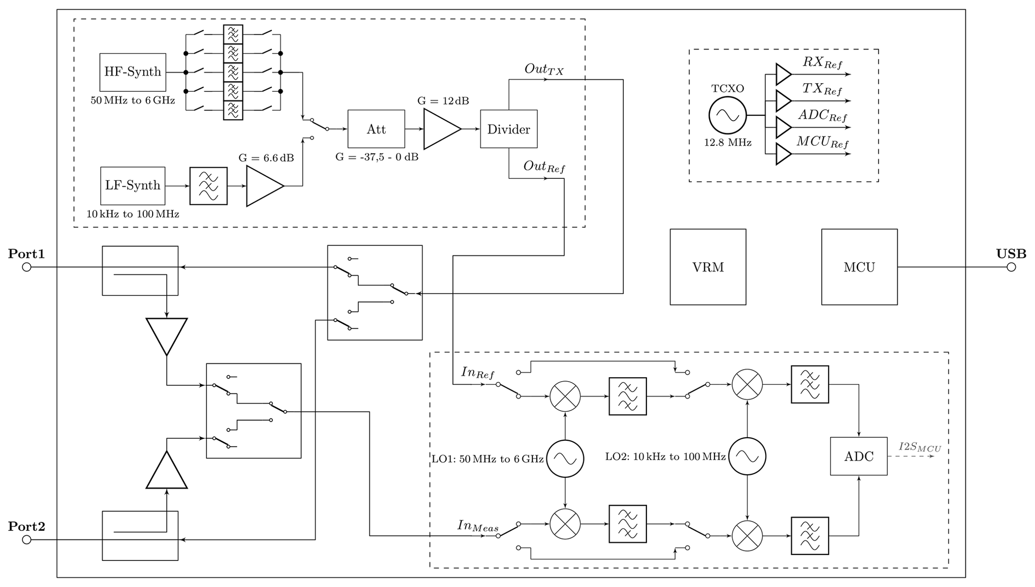
The device utilizes a single synthesizer, dual heterodyne receivers and two directional couplers, similar to the three receiver architecture from Dunsmore (2012), but with switched measurement ports. This introduces uncertainty at calibration but reduces design complexity and cost. Switching between ports is done by cascading RF switches to improve isolation. The switches are of absorbing type and unused ports are terminated into 50 Ω. Figure 1 shows a simplified block diagram.
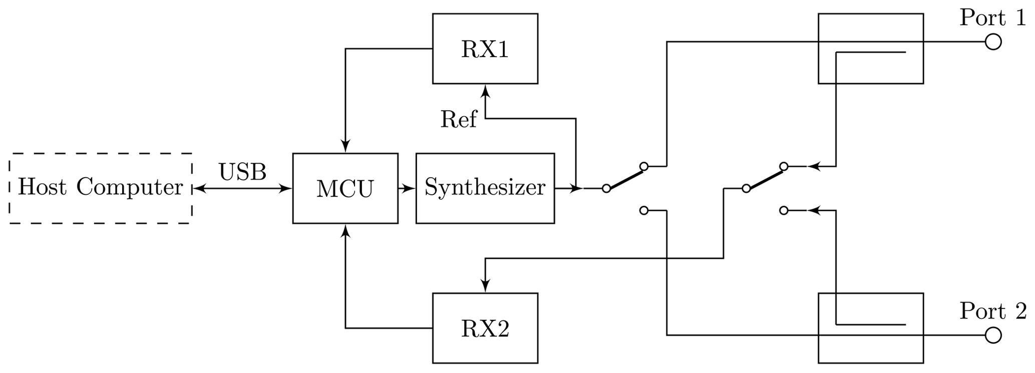
Synchronization of all elements is achieved through a shared 12.8 MHz reference clock supplied by a buffered temperature compensated crystal oszillator. The device is powered by a dedicated USB-Port through switching converters, although most blocks are supplied by local linear regulators to improve noise and spurious performance. A second USB port is being utilized for communication with a computer.
The final design utilizes a 4-layer printed circuit board (PCB) with a total size of 160 mm × 100 mm. The majority of components are mounted on the top side, while some parts of the synthesizer path are on the back. A cutout, pin-header and mounting holes for a Raspberry Pi are included in the design to allow standalone operation. Figure 2 shows the circuit board. Despite the higher loss described in Coonrod (2012), electroless nickel immersion gold finish with no solder stop on top of most RF traces was chosen to slightly improve impedance matching. As can be seen on the upper left section, minor modifications on the digital circuitry around the microcontroller were necessary.
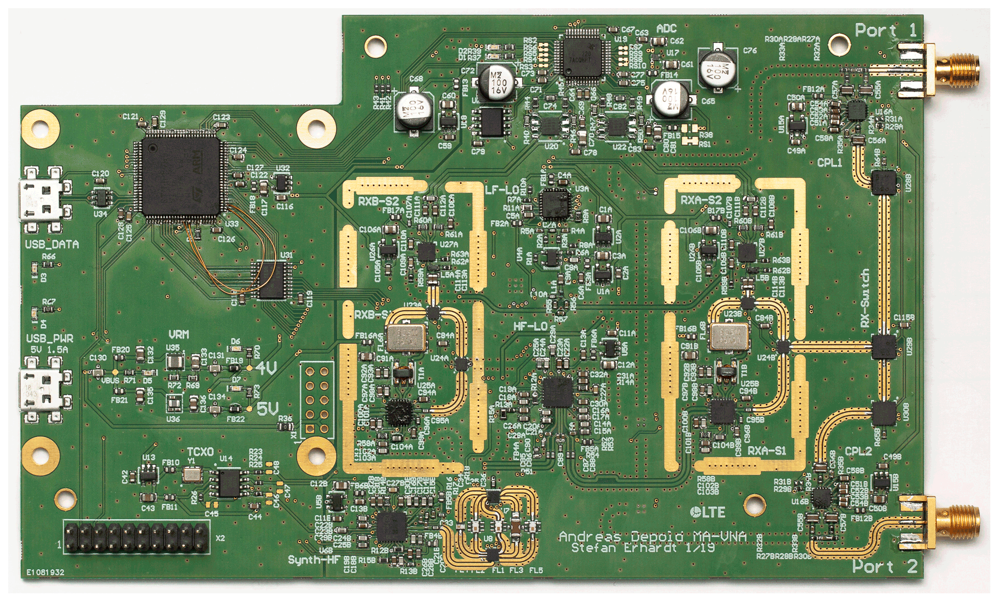
Figure 2Top side of the VNA circuit board. The two measurement ports are accessible through SMA connectors.
3.1 Synthesizer
The very wide frequency range from 10 kHz to 6 GHz is achieved by utilizing two independent sources. Frequencies above 50 MHz are generated by a Fractional-N phase-locked loop (PLL) with integrated voltage controlled oscillators (VCOs) and output dividers, a Maxim Integrated MAX2871 integrated circuit (IC). After generation the signal travels through one of five selectable ceramic low pass filters, of which the edge frequencies are staggered to minimize output distortion.
Lower frequencies are generated by a 250 MS/s Direct-Digital-Synthesis (DDS) IC, an Analog Devices AD9913. The output is amplified and filtered through a discrete LC network.
The source is selected through a RF switch which feeds the final output stage. This stage consists of a digitally controlled attenuator and a gain-block amplifier. Level control and power linearization is done in software by setting the attenuation through a look-up-table. The correction values have been acquired by characterization. The reference signal is split off after this stage by an unequal resistive divider. The lower frequency limit is governed by DC-blocking capacitors and the amplifiers bias circuitry.
3.2 Directive Elements
The device utilizes one directive element per port to split the incoming from the outgoing wave. They are based on a resistive Wheatstone bridge (Dunsmore, 1991), with the source and test port being single-ended. In low-cost devices the differential coupled output is commonly directly tied into a balanced mixer, as described in Colman et al. (2011). Due to receiver architecture and wide bandwidth requirements this design makes use of a fully differential amplifier instead. The schematic can be seen in Fig. 3.
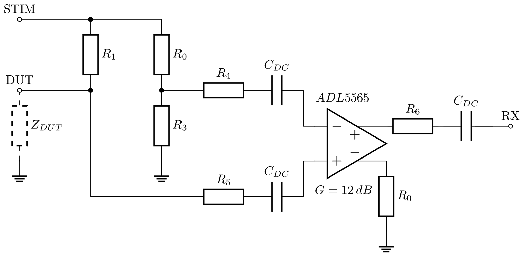
R1 and R3 form the actual bridge together with R0=50 Ω and ZDUT. It is only in balance when Eq. (1) is true. Instead of coupling the wave dependent on its source direction like for example microstrip couplers, this circuit's output is proportional to the mismatch of ZDUT to R0 achieving the same effect but at the cost of losses. Insertion loss and the proportional factor are determined by the relation of R1 and R3.
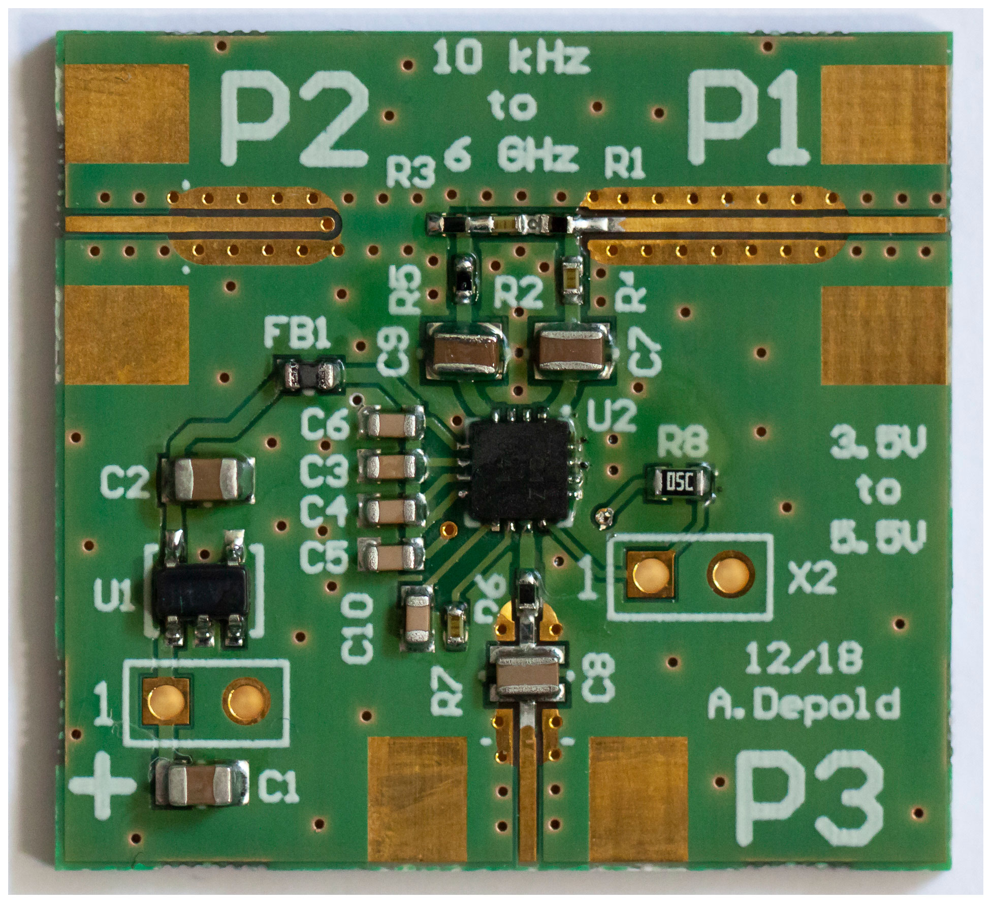
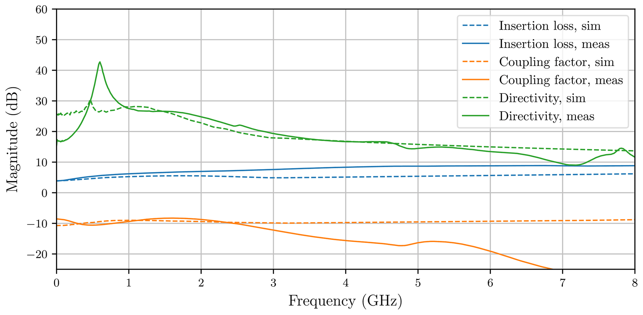
R4 and R5 improve the circuit's performance and were determined through simulation in Advanced Design System. Low series inductance flip-type capacitors were used as DC blocks to allow very high capacity without sacrificing high frequency performance. In Fig. 4 the evaluation board of the bridge can be seen. The design of this board is an exact replica of the circuit used on the analyzer itself. While the insertion loss of this particular design is substantial, especially at high frequencies, its very high bandwidth, small size and low-cost make it a good choice for a compact device. The design can be mirrored to ease the layout of RF traces on the PCB. The bridge was simulated and characterized independent of the whole system. In Fig. 5 the results are shown. Above 2 GHz the simulation should be seen with a grain of salt, as the manufacturer supplied S-parameters are not available for these higher frequencies.
3.3 Receivers
Both receivers are of identical two stage superheterodyne design. While the reference path does not require the same high dynamic range as the measurement path, identical design improves total accuracy as errors caused by some external factors, for example slight supply voltage fluctuations and temperature changes, are correlated. The first stage of the receivers utilizes an Analog Devices ADL5801 double balanced active mixer. The minimum input frequency of this stage is not limited by the lower specification of 10 MHz of the mixer, but by the intermediate frequency (IF) as approaching this frequency causes an effectively dead band. Bandwidth is limited to 30 kHz by a crystal filter centered at 45.00 MHz between the stages. While narrow band limiting is not necessary for network analysis as the input signal is a known sinusoid, this filter allows the device to be used as a rudimentary spectrum analyzer, although some band selection filtering should be done on the input side in this usage scenario to prevent reception of mirror frequencies.
The receivable frequency range is extended by allowing the entire first stage to be skipped. In this mode the input signal is directly fed into the second stage mixer without filtering. This stage also utilizes an active mixer to minimize total insertion loss through the receive chain.
As in the synthesizer, the high frequency local oscillator (LO) is a VCO/PLL, while the lower frequency is generated by a DDS. The combination of PLL/VCO and DDS LOs allows for very fine frequency control, as the resolution of the PLL is fairly low and can be off by up to 1 ppm at its lower frequency edge. All errors caused by this limited resolution of the PLLs in both the first receive stage as well as the synthesizer are accounted for and corrected in the second stage LO. No tracking of the signal during the digital-down-conversion step is needed.
3.4 Signal Processing and Software
The low IF signals are digitized by an audio ADC. These achieve high dynamic range and low distortion at a low cost, whereas the bandwidth is very limited. Both the measurement and the reference signal are captured simultaneously at a sample rate of 200 kS/s. The data is read by a STM32F7 microcontroller, buffered, and transferred to a computer via USB. Filtering, digital down-conversion and amplitude/phase extraction are done on the host utilizing Python, although the fast processor would allow this to be done on the device itself. Calibration is handled by the free Python library scikit-rf.
The VNA is controlled through a Qt-based graphical user interface (GUI), which handles the data management, calibration and visualization. All features needed for measurements are implemented within the GUI, including simple time domain analysis and a step-by-step calibration wizard supporting 1- and 2-ports and -Term error models. In a two receiver VNA design port characteristics can change when configuring the device for capturing of different S-parameters. Although the -Term calibration implementation in scikit-rf does attempt to determine these switch terms, some errors remain and will reduce measurement accuracy compared to a four receiver design without switches.
3.5 Final Design
To conclude the device description, Fig. 6 shows a more detailed block diagram. The synthesizer block shows the harmonic filtering as well as the power leveling architecture. Nominal output power of the generator block is 10 dBm resulting in a maximum port output power after losses in the switches and bridge of 0 dBm, which is held to about 1 GHz. In the receive direction total attenuation approaches 15 dB at higher frequencies which therefore results in −15 dBm typical receiver input power.
All measurements were taken with the circuit board as seen in Fig 2, unless otherwise noted. No case or additional shielding was used.
4.1 Characterization
In the following sections some characteristic data is shown followed by example and validation measurements. Where applicable calibration was performed with off-the-shelf shorting caps and terminations with no characteristic data. No open standard was utilized.
4.1.1 Dynamic Range
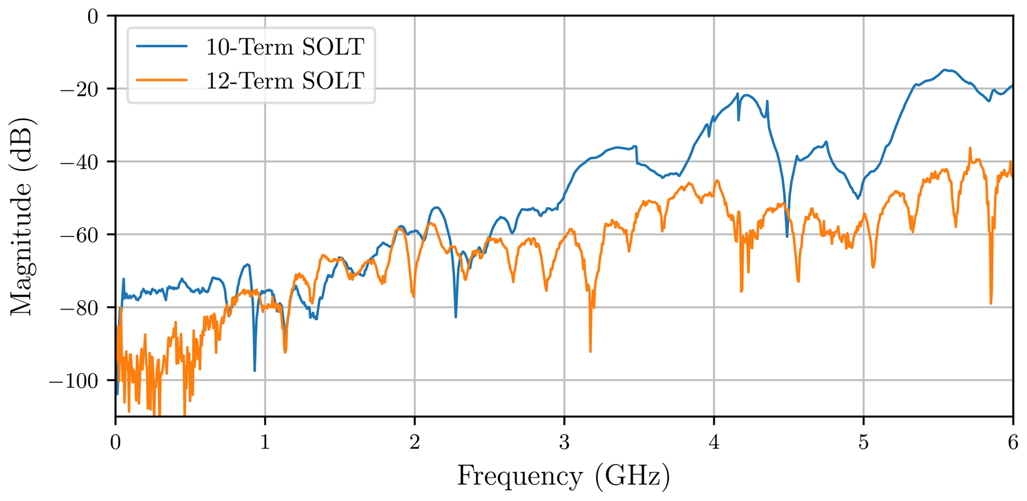
Dynamic range was determined by measuring S21 with both ports unconnected. Figure 7 shows the result using two different calibration techniques. 12-Term calibration decreases the noise floor, as some correlated crosstalk is corrected compared to the 10-Term algorithm. It is clearly visible that the device dynamic range is constrained by limited isolation rather than noise. Optimization of the layout and addition of shielding may enhance this greatly. Without modification of the hardware this may be improved by using fully specified calibration standards.
4.1.2 Port match
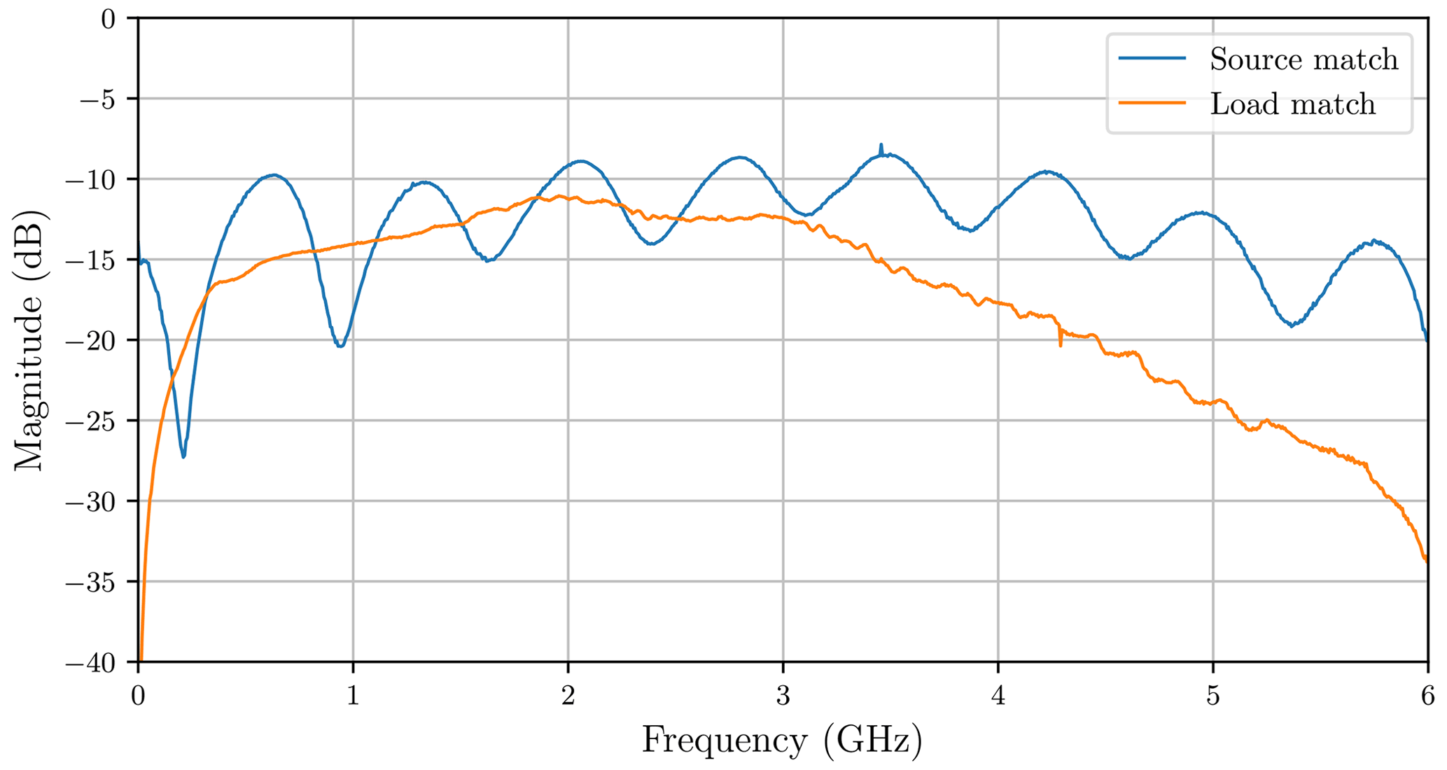
The physical port match of the device is governed by the complete signal chain from synthesizer or receiver to the actual SMA-port. As such it differs between the receive and transmit modes. Figure 8 shows the result for both cases. These can not be physically measured by an external device and therefore are determined through the error coefficients estimated during calibration using scikit-rfs 12-Term algorithm. Only port 1 is shown, as both ports behave very similarly. It should be noted that this result does not paint the complete picture for a two receiver VNA, as the ports characteristics are not only different for receive and transmit modes, but are also affected by the exact switch configuration. As such, this result should be viewed as only a general indicator of the port match, not as an exact result.
4.2 Measurements
Multiple evaluation measurements were conducted. For comparison a Rohde & Schwarz ZVB 8 was used, which in this case can be seen as a close to ideal reference measurement. It was calibrated using an automatic calibration unit.
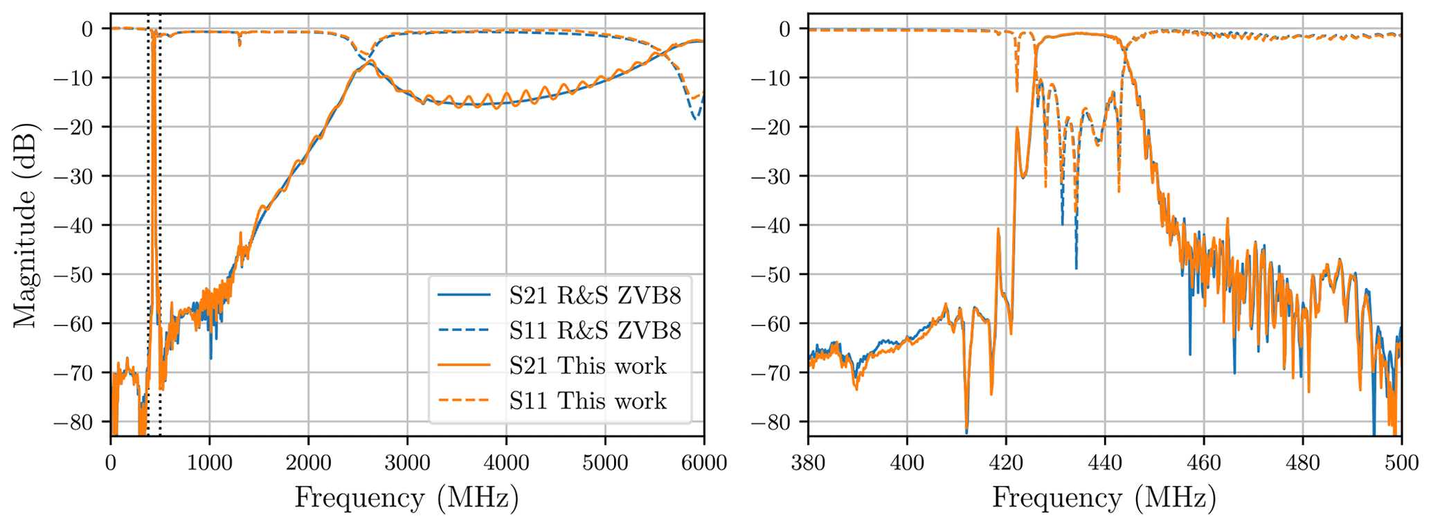
Figure 9 shows the measurement of a SAW bandpass filter. Around the passband of the 433 MHz bandpass filter the two graphs align almost perfectly. A prominent ripple is visible in the transmission graph of the device at higher frequencies. This is caused by use of less than ideal calibration standards, as no characterization data to correct for imperfections and electrical length was available.
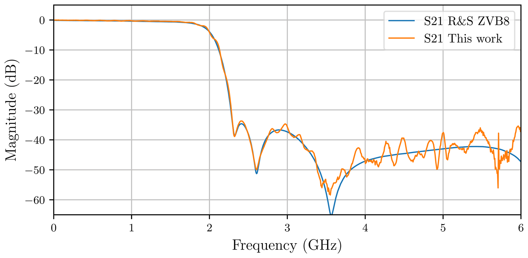
In Fig. 10 a Mini-Circuits VLF-1700 (Low pass filter, DC − 1700 MHz) can be seen. As in the previous case the passband and falling edge match almost perfectly between the two devices. The stopband measurement quality above 3.5 GHz is limited dominantly by crosstalk.
4.3 Final Specification
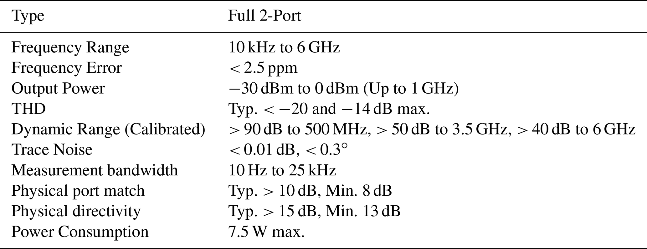
To summarize, the final specification can be seen in Table 1. Trace noise and measurement bandwidth lie in the typical span for low-cost VNAs, while dynamic range, frequency range and harmonic distortion are far better than commercially available low-cost devices.
A low-cost network analyzer with comparably high performance was successfully designed and implemented. In conclusion the presented device shows the viability of a low-cost vector network analyzer using only commercial off-the-shelf components. While continued work is needed to turn this device into a marketable product the foundation has been set.
Source code and measurement data are not publicly available. Inquire at the authors for further information.
AD and SE created the concept and architecture. AD designed and built the hardware, wrote the software and carried out the measurements. Editorial input was given by FL and RW.
The authors declare that they have no conflict of interest.
Publisher’s note: Copernicus Publications remains neutral with regard to jurisdictional claims in published maps and institutional affiliations.
This article is part of the special issue “Kleinheubacher Berichte 2020”.
This paper was edited by Thorsten Schrader and reviewed by Frauke Gellersen and Karsten Kuhlmann.
Colman, G., Bauwelinck, J., and Vandewege, J.: DC-coupled directional bridge front-end for vector network analyzer receiver in GHz-range, IEICE Electron. Expr., 8, 814–818, 2011. a
Coonrod, J.: Ambiguous Influences Affecting Insertion Loss of Microwave Printed Circuit Boards, IEEE Microw. Mag., 13, 66–75, 2012. a
Dunsmore, J.: Simple SMT Bridge Circuit Mimics Ultra-Broadband Coupler, in: RF Design magazine, 105–10, 1991. a
Dunsmore, J.: Handbook Of Microwave Component Measurements, John Wiley & Sons, Chichester, West Sussex, United Kingdom, p. 69, 2012. a