 | 04 Sep 2018
Humidity and temperature sensor system demonstrator with NFC tag for HySiF applications
Amro Eldebiky
Mourad Elsobky
Harald Richter
Joachim N. Burghartz
Hybrid System-in-Foil (HySiF) is one of the emerging branches of flexible electronics in which ultra-thin silicon chips are integrated with flexible sensors in polymeric foils (Elsobky et al., 2018; Alavi et al., 2018). Intensive attention was given to the implementation of flexible environmental sensing platforms for logistics and food packaging (Cartasegna et al., 2011; Liu et al., 2016). The aim of this work is the implementation of a sensor system demonstrator using HySiF components, namely an ultra-thin microcontroller chip in addition to an on-chip temperature and an on-foil humidity sensors. The measurement concept for the relative humidity sensor is measuring the capacitance difference between an off-chip (on the foil substrate) humidity dependent sensor capacitor, and another humidity independent reference capacitor. The electrical readout technique is based on the charge amplifier switched capacitor circuit. It is implemented using a commercially available microcontroller (EM microelectronics EM6819) which has the advantage of being available as single chips to enable post-processing steps such as backthining and chip embedding in a thin polymer package. Sensor and reference capacitors are homogeneously integrated on-foil. 400 and 30 µm thick microcontroller dies (MCU) are used in this application. The charge amplifier result is digitized using an internal 10-bit analog-to-digital converter (ADC). The 10-bit ADC is time multiplexed between the charge amplifier structure and the internal temperature sensor. Linear interpolation is used to fit the digital output of the ADC and calibrate the output of the sensor system. Readings of the humidity level and the temperature are written to an NFC tag (from the company EM microelectronics based on chip EM NF4) using the contact interface. Readings can be accessed using a customized android application on a smartphone.
- Article
(1909 KB) - Full-text XML
- BibTeX
- EndNote


Industry 4.0 is the term used to represent the fourth industrial revolution first proposed at Hannover fair (Zhou et al., 2015; Jazdi, 2014). Cyber-Physical System (CPS), and Internet of Things (IoT) represent the bases of Industry 4.0, which lead to what is known as the intelligent factory. Building a highly flexible production model of personalized digital products and services, with real-time interactions between people, products and devices is the main objective of Industry 4.0 (Zhou et al., 2015). ParsiFAl4.0, which stands for “Produktfähige autarke und sichere Foliensysteme für Automatisierungsösungen in Industrie 4.0”, is an Industry 4.0 research project, which aims to develop innovative sensor technology and electronics in thin plastic films with cooperation partners from industry and research (Parsifal 4.0., 2017). In this project, a demonstration of pneumatic drives and packaged goods can collect, evaluate and exchange information about the respective production process through flexible sensor labels. These smart labels are implemented by using flexible sensors and circuit elements, as well as technological approaches like HySiF.
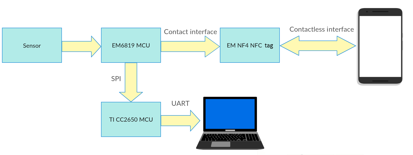
Figure 1MCU based system overview: A readout technique for the sensor based on the charge amplifier circuit is implemented using the available resources of the EM6819 MCU, and switching techniques programmed on the MCU. The MCU processes collect readings from the humidity sensor, and the reading of the internal temperature sensor and sends readings to the EM NFC tag on a contact serial interface. Measurements are read from the NFC tag using an android application developed at IMS CHIPS on a smartphone. Sending the data to the PC is done using the UART interface of the PC and using the TI CC2650 MCU as a converter from SPI to UART.
The main objective of this work is the design and implementation of a sensor system demonstrator for environmental quantities (humidity and temperature) using HySiF components, namely an ultra-thin microcontroller chip, on-chip temperature, and on-foil humidity sensors. As Fig. 1 shows the system structure, the on-foil humidity sensor is interfaced with the ultra-thin EM6819 MCU used to implement the readout of the humidity sensor. Measurements of the humidity sensor and the internal on-chip temperature sensor are written to an NFC tag accessed by an android application on a smartphone, and also sent to a PC and plotted in real-time application. Sending the data to the PC is done using the UART interface of the PC and using the TI CC2650 MCU as a converter from SPI to UART (EM6819 MCU does not have a UART interface). This is a step in the process of the smart labels of the Parsifal 4.0 project, and on the road of enabling flexible electronics for applications of industry 4.0. The structure of the on-foil humidity sensor is explained in Sect. 2. Additionally, Sect. 3 discusses the implementation of the readout circuit using the EM6819 MCU resources and overviews its architecture. Section 4 discusses the characterization of the sensor system and results. Finally, Sect. 5 concludes the main findings of this work.
Humidity sensors measurement concept is generally one of two alternatives: either capacitive, or resistive. For the capacitive approach, the relative humidity value is determined based on the change of the capacitance of the sensor as the dielectric constant of the sensing material is dependent on the relative humidity value.
In this work, capacitive humidity sensors are used. In addition, the capacitance reading is done as a differential measurement between a humidity sensor capacitor, and another humidity independent reference capacitor (Elsobky et al., 2017). The structure of the capacitive sensors used in this work is the interdigitated fingers structure (shown in Fig. 2) due to its simplicity to be integrated in our foil system (1 metal layer). Different finger widths and spacings are fabricated and characterized ranging from 5 to 20 µm with metal thickness from 2 to 5 µm in a fixed area of 5 mm×5 mm. The used material whose relative permittivity change with relative humidity level is Durimide (Fujifilm Electronics Materials). The material is spin-coated on the interdigitated structure of the sensor at speed of 1500 rpm, and baking temperature of 250 ∘C. The achieved thickness is from 2 to 5 µm (Elsobky et al., 2017). The main difference between the sensor and the reference capacitors is that the reference capacitor is covered with a Benzocyclobutene (BCB) layer in order to make it insensitive to the variation in the humidity level.
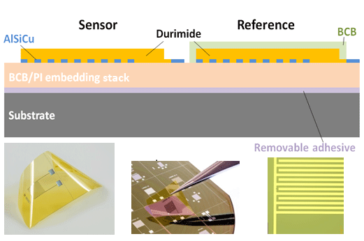
Figure 2On-foil interdigitated humidity sensor and reference capacitor structure. Both capacitors have identical structure with the reference capacitor covered with additional BCB layer (Elsobky et al., 2017).
The implemented approach for interfacing with the flexible capacitive sensor is a microcontroller based readout technique. The sensor readout is implemented using EM6819 microcontroller resources (Operational Amplifier (Op-Amp), 10-bit analog to digital converter (ADC), serial peripheral interface (SPI), timer, interrupt request controller, and general purpose input/output pins (GPIO)) with a switching mechanism that will be discussed in this section. The internal bandgap temperature sensor is used to get the temperature reading with the typical range for the operation of the EM6819 MCU is from −40 to 85 ∘C. The ADC configuration is time multiplexed between the charge amplifier structure for the humidity reading and the temperature sensor. The EM6819 is a microcontroller designed to be battery operated for extended lifetime applications. It has a large voltage range from 3.6 V down to 0.9 V (3-V battery operated in this application for autonomous operation). It has an 8-bit RISC architecture specially designed for very low power consumption (EM Microelectronic- Marin SA., 2014).
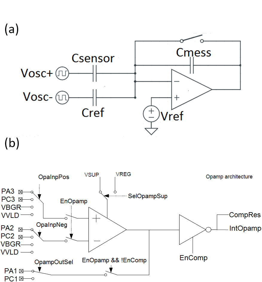
Figure 3(a) charge amplifier circuit. (b) EM 6819 Op-Amp connections overview (EM Microelectronic- Marin SA., 2014).
3.1 Charge Amplifier Circuit Structure
The readout circuit depends on the charge amplifier switched capacitor circuit using an Op-Amp (Fig. 3a). It measures the capacitance difference between two capacitors connected in a half bridge configuration where the charge difference between the sensor capacitor (CSensor) and the reference capacitor (CRef) is sampled on the sampling capacitor (CMess). The circuit switches between two states. The first state is the reset phase, and the second one is the sampling phase. The reference voltage of the charge amplifier represents the analog output voltage for the case of zero capacitance difference measured (ΔC=0) (common mode voltage). The feedback capacitor (CMess) defines the maximum capacitance difference that can be measured, and the sensitivity of the circuit to ΔC. During the reset phase, no ADC conversion is run and the feedback capacitor is shorted to return to the reset phase. The analog output of the Op-Amp in this case is the common mode voltage connected to the positive input of the Op-Amp. When the circuit switches to the sampling phase, the analog output is connected to CMess. CMess is applied in the feedback (no short circuit), and ADC conversion can take place after next toggle of Vosc+ and Vosc− to get the digital reading. The analog output voltage is defined by:
3.2 EM6819 Operational Amplifier Structure
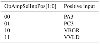
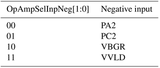
Figure 3b shows connections overview of the EM6819 Op-Amp. Each pin of the Op-Amp in EM6819 can be connected to different GPIOs, or other peripherals of the EM6819 microcontroller. These connections are programmed by adjusting the corresponding bit in the Op-Amp configuration registers. The positive input selection is done with OpAmpSelInpPos[1:0] in register RegOpAmpCfg2[7:0] as shown in table 1.
The negative input selection is done with OpAmpSelInpNeg[1:0] in register RegOpAmpCfg2[7:0] as shown in Table 2.
When the Op-Amp is enabled, the output can be mapped on to different GPIOs with OpAmpSelOut in register RegOpAmpCfg2[3] as shown in Table 3.
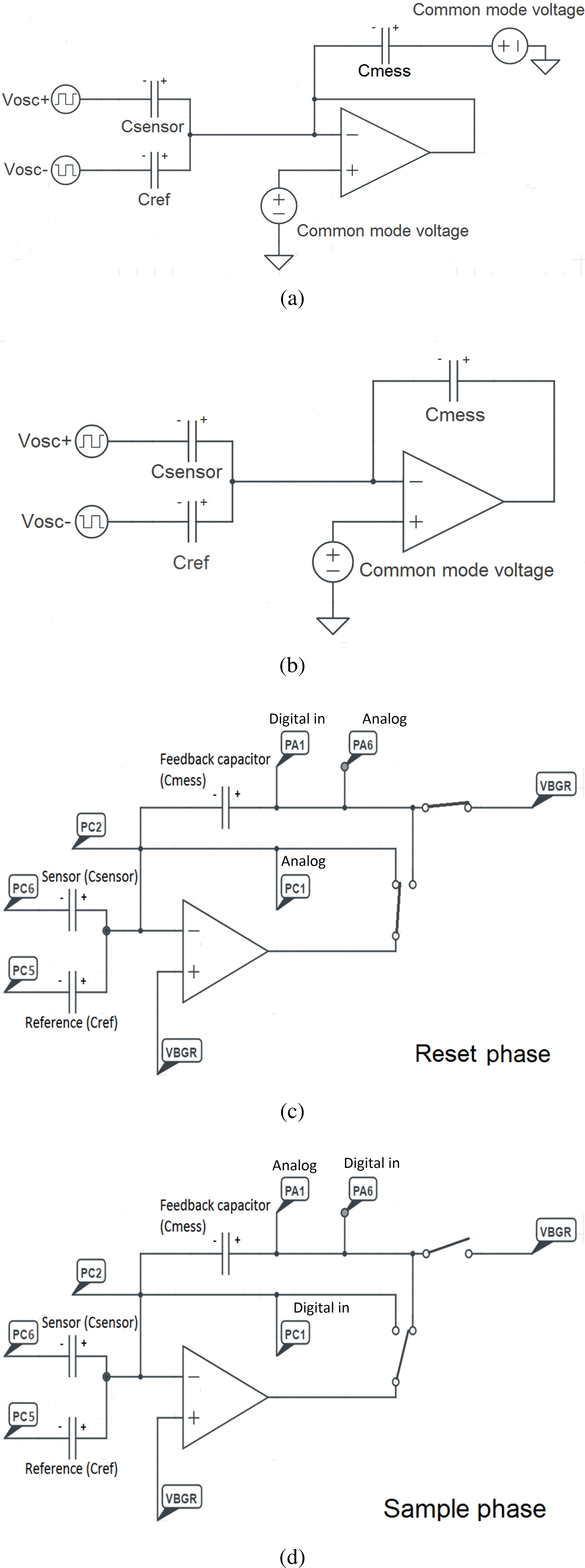
Figure 4(a) EM6819 charge amplifier reset phase. (b) sample phase. (c) Charge amplifier reset phase mapped on EM6819 resources. (d) sample phase.
By comparison between the available architecture as Fig. 3 shows, and the intended structure and functionality, it is achieved by dividing the problem into two phases:
-
Reset phase: Figure 4a shows the circuit structure during the reset phase and how it is mapped to EM6819 resources and pin assignment in Fig. 4c:
-
The feedback capacitor must be reset – its positive terminal must be connected to virtual ground in order to discharge (Q=CV).
-
The Op-Amp output is not connected to the ADC for sampling (no conversion takes place), but connected to its negative input terminal in feedback, and the structure can be shown as in Fig. 4a.
-
-
Sampling phase: Figure 4b shows the circuit structure during the sampling phase and how it is mapped to EM6819 resources and pin assignment in Fig. 4d:
-
The feedback capacitor must be connected between the two different terminals of the negative input, and the output of the Op-Amp.
-
The Op-Amp output is no longer connected to its negative input, and is connected to the input of the ADC (the conversion takes place after the next toggle).
-
Vosc+, and Vosc− are implemented using two GPIO pins as digital outputs that toggle periodically based on the timer interrupt. The timer full value is set depending on the required period for the square wave excitation of the half bridge, so that Vosc+, and Vosc− are 3 and 0 V alternatively with the required phase shift of the 180∘. PC5 and PC6 pins are used for this purpose, so the negative terminal of the reference capacitor is connected to PC5 (Vosc−), and the negative terminal of the sensor capacitor is connected to PC6 (Vosc+). The positive terminal of each capacitor needs to be connected to the negative input of the Op-Amp. PC2 is used as the negative input GPIO pin of the Op-Amp (Table 2), so the positive terminal of the reference and the sensor are connected to PC2 together.
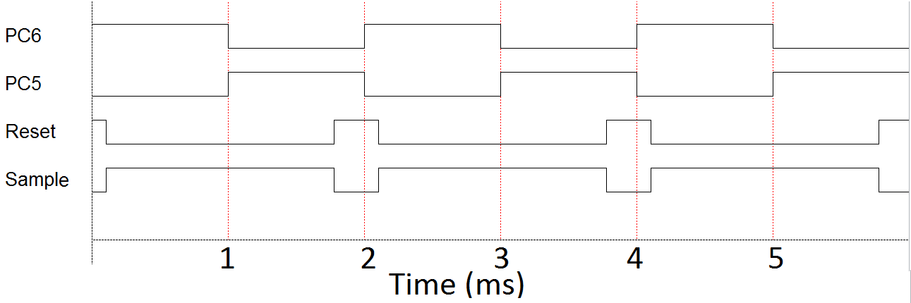
Figure 5If the pin PC6 (Vosc+) is high, then the sample phase must be applied, and wait for the next edge (toggle), and if it is low (the wait for the next toggle is over) then we start acquisition of the ADC reading as explained, and accumulating the acquired reading on the sum, then the reset phase setup is applied.
The positive input of the Op-Amp is the common mode voltage for the amplifier circuit which is supposed to be Vsup∕2 for symmetric operation of the readout circuit. However, in our application the internal bandgap reference voltage (VBGR=1.236 V) is used as the common mode voltage for the Op-Amp due to the absence of integrated Vsup∕2 voltage. This change in value of common mode from Vsup∕2 (1.5 V) to 1.236 V causes a shift of the mid-range result of the capacitance difference ΔC=0, and is discussed in demonstration and results section. These previous connections are the same for the reset phase and the sampling phase, so no switching occurs for these pins.
Thus, the two nodes which are switched between the two states are the positive terminal of the feedback capacitor, and the output node of the Op-Amp. In order to map these two nodes to match the available structure of the EM6819 microcontroller, the positive terminal of the feedback capacitor is connected to two shorted GPIO pins of the microcontroller. One of them is available as the analog bandgap reference voltage output, while the other one is available as the output node for the Op-Amp. After reference to Table 3 we chose PA1, and PA6 (which is available as VBGR output).
Concerning the output of the Op-Amp, after reference to Table 3, the two available options are PA1 and PC1. PA1 is available as ADC analog input, so it will be assigned to the Op-Amp output during sampling, and to the ADC input by adjusting the bits ADCSelSrc[2:0]. The second choice for the Op-Amp output PC1 is assigned to the Op-Amp output during the reset phase, and the GPIO pins PC1 (Op-Amp reset phase output), and PC2 (Op-Amp negative input terminal) are short circuited on hardware connection to get the short circuit feedback discussed above. Figure 5 shows the non-overlapping timing scheme for switching between the reset phase and the sample phase. When switching between two pins, we have to set one of them as high impedance (digital input), and then enable the functionality of the other, in order to avoid two nodes shorted on each other, and each one is trying to drive the pin. Figure 6 shows the program flow which can be divided into two parts:
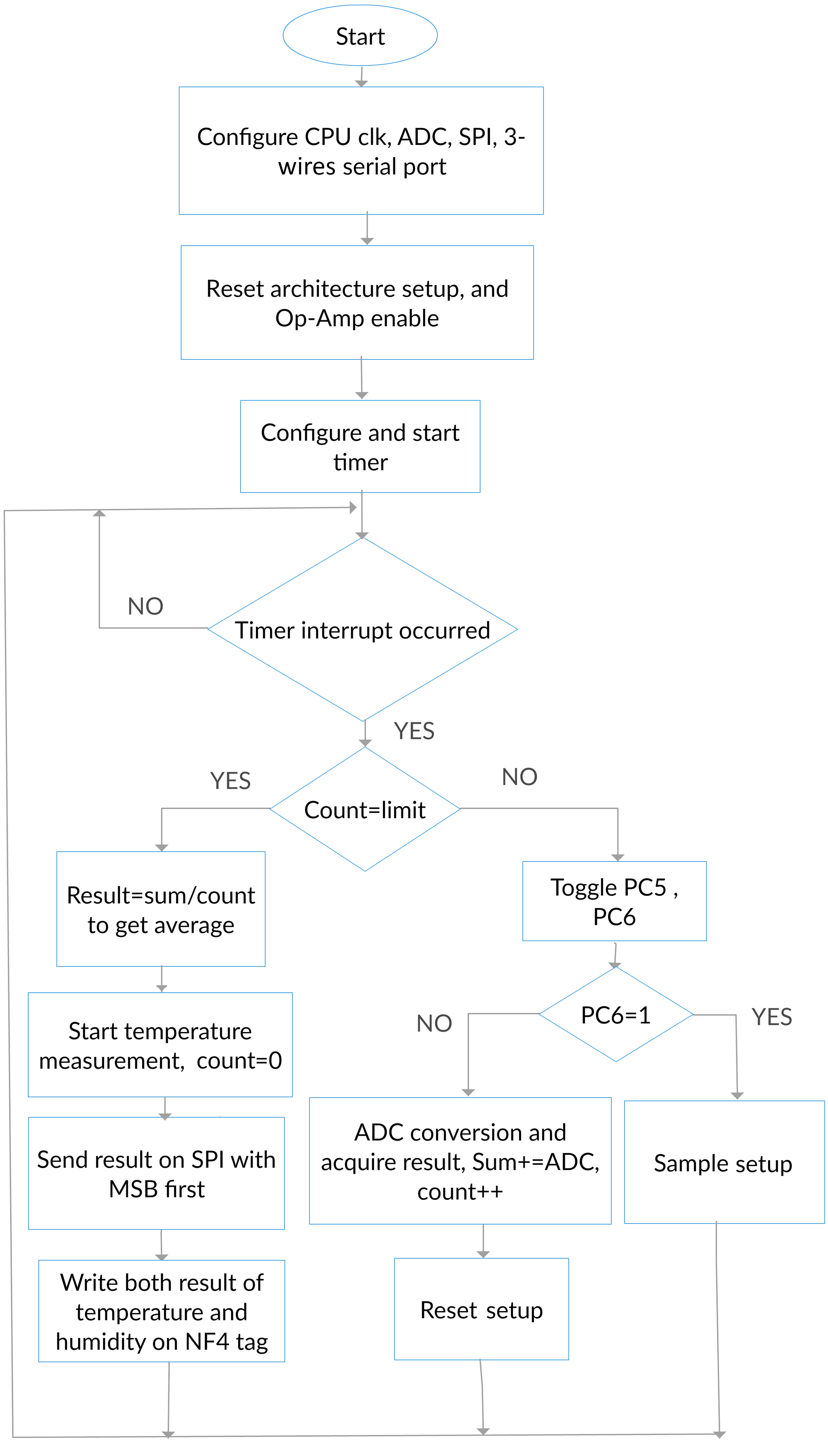
Figure 6EM6819 program algorithm flowchart: At start of the program initial setup is done for all used peripherals, and then in every periodic call of the interrupt handler we check to see whether the required number of capacitance difference measurements is reached or not. If it is reached, then the average is calculated, the ADC is configured for initiating temperature sensor measurement, and then both the average of the 10-bit reading of the capacitance difference, and the temperature reading in Celsius degrees are written on the NFC tag. The average is also sent on the SPI interface. If the number is not reached yet, we complete our measurements cycles.
-
The setting of the microcontroller environment.
-
The periodic acquisition of the results, averaging and displaying.
This periodic part of the program is done in the context of the interrupt request handler of the timer full value interrupt. The functionality of this periodic interrupt is to gather 10 (programmed changeable number) digital readings of the output of the charge amplifier, and then send the average of these readings, with the current temperature reading at this time to both: the NF4 tag (using the 3-wires contact interface), and the TI CC2650 microcontroller using SPI interface. The TI CC2650 is then used to send the received data to the PC on UART. The data is sent to the PC in this indirect way, because the EM6819 does not have a UART peripheral, so in order to be able to plot readings in real time and save readings in a file on the PC, the TI CC2650 is used as a converter from SPI to UART. If the number was not reached yet, we complete our measurements. The PC6, and PC5 GPIO pins are toggled, and the timing diagram in Fig. 5 is followed.
4.1 Humidity Sensor Characterization in Controlled Climate Chamber
A controlled climate chamber (Vötsch VCL 0010) is used to vary the relative humidity level with steps of 5 % at temperature of 30 ∘C while the humidity capacitive sensor L10S20 (interdigitated with finger width of 10 µm and finger spacing of 20 µm – area 5 mm×5 mm) is placed inside it. The sensor is connected during this experiment to the LCR meter (HEWLETT PACKARD 4284A Precision LCR Meter, 20 Hz to 1 MHz) in a four point measurement setup in order to measure the capacitance with different humidity levels. As Fig. 7 shows, the recorded points of measurement are then linearly fitted in MATLAB to find a linear fit () and check the goodness of this fit by calculating R-square, Root mean squared error (RMSE), and The Sum of Squares due to Error (SSE).
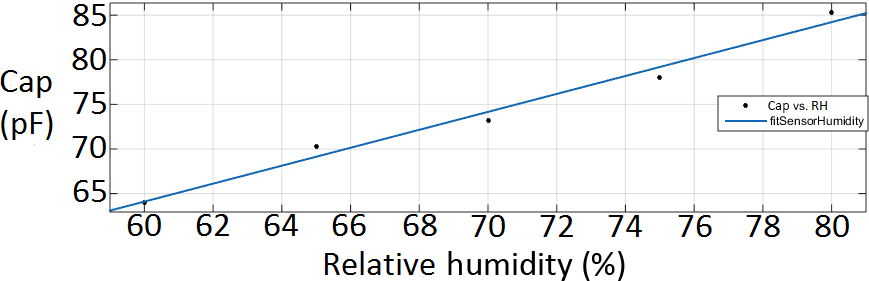
Figure 7Capacitance readings of the sensor characterization in the climate chamber linear fit: coefficients (with 95 % confidence bounds): . Goodness of fit: , R-square=0.9811, Adjusted R-square=0.9748, .
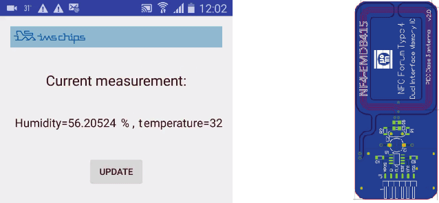
Figure 8Near field communication (NFC) tag based on EM NF4 chip, and android application developed to access readings written to the NFC tag.
4.2 Graphical User Interface
In this demonstration, two methods are used in order to display the obtained results of the system:
-
Real-time plot of the data sent on UART to a PC using MATLAB. The baud rate is 9600 while the delay of the update of the screen is set to 0.01 s. The program also writes the time and data vectors history to a file so that it can be used for analysis.
-
NFC tag based on the NF4 chip by the company EM microelectronics. The NFC tag is read by an android application on a smartphone as shown in Fig. 8.
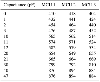
Table 4The ADC results of the circuit characterization experiment.
4.3 MCU based Readout Static Characterization
In order to characterize the performance of the charge amplifier structure, an experiment is conducted using discrete circuit elements on a breadboard. Single capacitance measurement is done instead of capacitance difference measurement. The value of the capacitance is changed by connecting many discrete capacitors in parallel, and also changing the values of the connected capacitors. The value of the ADC output was recorded at each value of the capacitance by displaying it on the PC. Different MCUs are used in this experiment in order to notice the difference in performance between the different units. The value of the feedback capacitor in this experiment is 47 pF. Table 4 shows the results for three different MCUs. The MCU wafer was originally 200 mm in diameter. A 150 mm-diameter wafer is cut out of it after that. Next, a 10 nm-thick titanium layer is deposited by sputtering. The next step is deposition of a 100 nm-thick titanium nitride layer also by sputtering. Lithography process and dry etching is then applied to the wafer. Finally, it is annealed at 400 ∘C temperature in nitrogen for an hour, and for 30 min in hydrogen. The three MCUs differ in the order of processing steps they experience. The first MCU (MCU 1) was thinned to 400 µm, and then annealed for reconstruction. The second MCU (MCU 2) was first annealed, and then thinned to 400 µm. The third MCU (MCU 3) was thinned to 400 µm and was not annealed.
As noticed from Table 4, the effective number of bits is reduced to about 9.78 and the mid-range (ΔC=0) value is shifted below 512 because of the usage of the internal bandgap reference voltage (VBGR=1.236 V) as the common mode voltage of the Op-Amp due to the absence of an integrated Vsup∕2 voltage. The dynamic range is typically from 0 V to about 2.6 V (the highest effective number of bits for the ADC can be obtained for Vsup=2.6 V). The obtained results are analyzed using the curve fitting tool on MATLAB to check the linearity of the results as a sign of the performance of the implemented approach. The tool is used to get a linear model () to fit the readings of each MCU. Figures 9, 10, and 11 respectively show the obtained results of each tested MCU. As an indication of the goodness of the linear fit, RMSE, SSE, R-square, and Adjusted R-square are calculated.
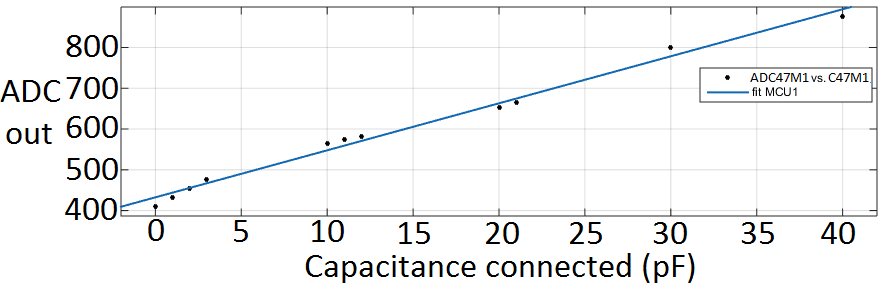
Figure 9The circuit characterization ADC result linear fit for MCU 1: coefficients (with 95 % confidence bounds): . Goodness of fit: SSE=2281, R-square=0.9899, Adjusted R-square=0.9887, RMSE=15.92.
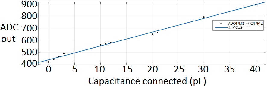
Figure 10The circuit characterization ADC result linear fit for MCU 2: coefficients (with 95 % confidence bounds): . Goodness of fit: SSE=1476, R-square=0.9933, Adjusted R-square=0.9926, RMSE=12.81.
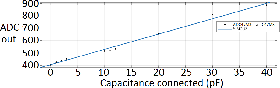
Figure 11The circuit Characterization ADC result linear fit for MCU 3: coefficients (with 95 % confidence bounds): . Goodness of fit: SSE= 2557, R-square=0.9901, Adjusted R-square=0.989, RMSE=16.85.
Good linearity is achieved in all demonstrators samples with minimum realized R-square (coefficient of determination) is 0.9899. It is observed from the three figures that every set of neighbouring points shows a very linear manner, so the source of the non-linearity between some non-neighbouring points originates from the mismatch in the external discrete capacitors which introduces some error. Besides, the different parasitic capacitances between the different nodes of the breadboard and due to the connections between the capacitors and the MCU pins can cause errors.
4.4 Dynamic Characterization of the Complete System in Controlled Climate Chamber
The controlled climate chamber (Vötsch VCL 0010) is used in an experiment in order to characterize the complete system performance by varying the relative humidity value inside the chamber. The relative humidity value is varied from 50 %–65 % with a step of 5 % while the temperature is kept constant at 30 ∘C. Both the sensor and the reference capacitor are placed inside the chamber and connected to the EM6819 MCU outside. In addition, the value of the used feedback capacitor is 100 pF. The timing duration of each humidity level from 50 %–65 % is 20 min and the duration of each ramp between any two levels is also twenty minutes. The used MCU in this experiment is one from type 1 that was thinned to 400 µm and then annealed. The ADC output at each humidity level is sent to a PC and written to a text file for further analysis using MATLAB. As Table 5 shows, the recorded ADC values are read from the written files for analysis and the average value of the ADC output is calculated as a representative for the ADC output at each humidity level.
Table 5The average of the EM6819 ADC output at each humidity level.
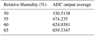
Next these obtained average values are used to check the linearity of the performance of the complete system and to get a linear model () to fit these values. As an indication of the goodness of the linear fit, RMSE, SSE, R-square, and Adjusted R-square are calculated. As Fig. 12 shows the results, quite good linearity is observed. However, the first calculated points at 50 %, 55 %, and 60 % humidity levels respectively show a very linear behavior. On the other side, the 65 % point is below this observed line. This can be explained by taking into consideration that at higher relative humidity the reference capacitor begins to increase. As a result, a lower difference than the expected (the linear fit of the first three points) between the sensor and the reference is observed in the output of the ADC. Figure 13 shows the linear fit with the 50 %, 55 %, and 60 % (excluding 65 % point).
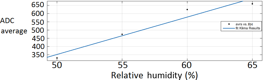
Figure 12The average values of the ADC result linear fit in chamber experiment: coefficients (with 95 % confidence bounds): . Goodness of fit: SSE=3666, R-square=0.9463, Adjusted R-square=0.9194, RMSE=42.81.
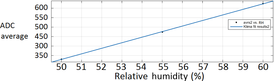
Figure 13The average values of the ADC result linear fit in chamber experiment excluding 65 % point: coefficients (with 95 % confidence bounds): . Goodness of fit: SSE=6.165, R-square=0.9999, Adjusted R-square=0.9997, RMSE=2.483.
In this work, an environmental sensor system (temperature and humidity) demonstrator for Hybrid Systems-in-Foil (HySiF) application is implemented using a MCU based readout approach. The circuit structure is implemented using the peripherals of the EM6819 MCU (Op-Amp, GPIO pins, and ADC) with a supply of 3 V and can be readily embedded in foil. An algorithm for switching between the reset and sample phases of the charge amplifier is implemented. The circuit is characterized by using discrete capacitances. Good linearity is observed in the operation region (coefficient of determination=0.9933). The charge amplifier structure is then tested with the on-foil sensor and reference capacitors. The ambient temperature is measured using the internal temperature sensor of the MCU. Two display methods are implemented using an NFC tag and MATLAB real-time plot on a PC. A serial interface for the communication with the NF4 chip is implemented using EM6818 GPIO pins. Readings are written to the tag, and then are read by the user through an android application on a smartphone.
The measurement data are available at: https://data.mendeley.com/datasets/fjn2dtckvh/draft?a=494e2410-c89a-4831-968e-20c2d8d5918b (last access: 17 August 2018).
The authors declare that they have no conflict of interest.
This article is part of the special issue “Kleinheubacher Berichte 2017”. It is a result of the Kleinheubacher Tagung 2017, Miltenberg, Germany, 25–27 September 2017.
We gratefully acknowledge the German Federal Ministry of Education (BMBF) for
financial support with the project Parsifal 4.0 (Project
ID.16ES0435).
Edited by: Dirk
Killat
Reviewed by: Ulrich Hilleringmann and one anonymous referee
Alavi, G., Sailer, H., Albrecht, B., Harendt, C., and Burghartz, J. N.: Adaptive Layout Technique for Microhybrid Integration of Chip-Film Patch, IEEE T. Compon. Pack. T., 8, 802–810, 2018. a
Cartasegna, D., Conso, F., Donida, A., Grassi, M., Picolli, L., Rescio, G., Malcovati, P., Perretti, G., and Regnicoli, G.: Integrated microsystem with humidity, temperature and light sensors for monitoring the preservation conditions of food, IEEE Sensors Conference, 28–31 October 2011, 1859–1862, 2011. a
Elsobky, M., Albrecht, B., Richter, H., Burghartz, J. N., Ganter, P., Szendrei, K., and Lotsch, B. V.: Ultra-thin Relative Humidity Sensors for Hybrid System-in-Foil Applications, IEEE Sensors Conference, 29 October–1 November 2017, 1–3, 2017. a, b, c
Elsobky, M., Mahsereci, Y., Yu, Z., Richter, H., Burghartz, J. N., Keck, J., Klauk, H. and Zschieschang, U.: Ultra-thin smart electronic skin based on hybrid system-in-foil concept combining three flexible electronics technologies, in Electron. Lett., 54, 338–340, 2018. a
EM Microelectronic- Marin SA: Sub-1V (0.6V) 8bit Flash MCU DC-DC Converter, E2PROM, available at: http://www.emmicroelectronic.com/, last access: 28 August 2017. a, b
Jazdi, N.: Cyber physical systems in the context of industry 4.0, IEEE Int. Conf. Auto., 22–24 May 2014, 1–4, 2014. a
Liu, X., Valente, V., Zong, Z., Jiang, D., Donaldson, N., and Demosthenous, A.: An implantable stimulator with safety sensors in standard cmos process for active books, IEEE Sens. J., 16, 7161–7172, 2016. a
Parsifal 4.0 project: available at: http://www.parsifal40.de/html/projekt.html, last access: 18 July 2017. a
Zhou, K., Liu, T., and Zhou, L.: Industry 4.0: Towards future industrial opportunities and challenges, Fuzzy Systems and Knowledge Discovery (FSKD), 12th International Conference, 15–17 August 2015, 2147–2152, 2015. a, b