 | 04 Sep 2018
A digital receiver signal strength detector for multi-standard low-IF receivers
Tobias Saalfeld
Tobias Piwczyk
Ralf Wunderlich
Stefan Heinen
This paper presents a receiver signal strength detector based on a discrete Fourier transform implementation. The energy detection algorithm has been designed and measured using a custom multi-standard transceiver ASIC with a low-IF receiver at 0.5, 1 and 2 MHz IF. The proposed implementation directly processes the single bit ΔΣ modulator data and features a clear channel assessment for arbitrary modulation schemes without energy consuming demodulation. Continuous monitoring of the derivative of the RSSI takes advantage of faster coefficient convergence for higher power levels and reduces computation time. A dynamic range of 65 dB has been achieved in FPGA based measurements with a linearity error of less than 1.2 dB. Furthermore, synthesis results for an on-chip implementation for an 130 nm RF CMOS technology show an overall power consumption of 1.5 mW during calculation.
- Article
(255 KB) - Full-text XML
- BibTeX
- EndNote


Short range wireless systems with low power consumption are increasingly used for communication of sensor networks. The communication of these networks usually takes place on three bands, which are also used for a various range of common standards. WiFi, Bluetooth or Bluetooth LE are located in the 2.4 GHz band or IEEE 802.15.4 (2016), which specifies multiple physical layers not only for 2.4 GHz, but also for 868 MHz and even for the 433 MHz ISM band. In the last decade all these bands have been increasingly occupied by various communications. Additionally, the trend of the recent years is going towards multi-mode, multi-standard transceivers which offer a wide range of functionality.
With the increased unlicensed use of these bands by various standards, listen
before talk functionality is getting more important to ensure a reliable
communication. These Clear Channel Assessments (CCA) can be run
based on the energy detected in a channel. For standards like
IEEE 802.15.4 (2016) a receiver energy detection (ED) is mandatory and a
corresponding value between 0x00 and 0xFF has to be
provided to the user. Furthermore, an accuracy of at least ±6 dB
is required to fulfill the specification.
The low-IF receiver (RX) architecture with ΔΣ modulators (ΔΣM) is a suitable solution for multi-standard operation due to its high reconfigurability (L. Zhang et al., 2013) and a high dynamic range (DR). The high DR relaxes the requirements of the analog front-end (Ho et al., 2011) by reducing the need for high gain as well as a fine tuning of analog gain. Even coarse gain steps in the RF front-end ensure a sufficient signal level at the analog-digital converter (ADC) input and the sensitivity specifications for a standard like IEEE 802.15.4 (2016) can be fulfilled. Accordingly, the automated gain control (AGC) loop of the RX front-end alone does not need a high resolution and can easily be controlled from digital signal processing. One method to determine the receiver signal strength indicator (RSSI) value with a high resolution can be found in the digital AGC loop of the digital baseband (BB) filters. However, these BB filters have a comparatively high current consumption during operation and the digital AGC has a build in hysteresis.
Common single band transceiver architectures like the one presented by Raja et al. (2010) or even the Atmel AT86RF233 (2014) use limiting amplifiers (LA) in the RX front-end to limit the signal amplitude to the DR of the ADC. LA offer the possibility of extracting the RSSI with a rather low additional effort as shown by Huang et al. (2000), but the reception of amplitude modulated signals is not possible in this case. However, in low-IF RX architectures like the one presented by Zolfaghari et al. (2017), LAs are not needed. Consequently, an energy and area efficient solution for the ED, instead of limiting amplifiers, is necessary.
This work presents a digital implementation for RSSI calculation based on a discrete Fourier transform algorithm without area consuming digital multipliers. Furthermore, the RSSI quality is monitored during RSSI calculation to minimize the computation time. The algorithm directly processes the oversampled ΔΣM single bit output data without previous digital filtering. Since the Fourier transform is a highly selective filter itself, down conversion, filtering, demodulation and decimation of the digital BB processing can be deactivated, if the received data is dispensable. This is the case in CCA-ED operation where it has to be ensured that the desired channel is not occupied. Hence, listen before talk functionality can be implemented in an energy efficient way by deactivating digital system components with high power consumption.
The presented RSSI calculation has been designed and tested using synthesized VHDL code executed on an FPGA and connected to a custom triple-band multi-standard transceiver ASIC. An overview of the used RX front-end, the requirements for energy detection and the implementation will be given in the following sections. Subsequently, the RSSI calculation algorithm will be discussed in detail and solutions for an area efficient implementation are given. Furthermore, the measurement setup is presented and the results are shown and compared to analog implementations of ED.
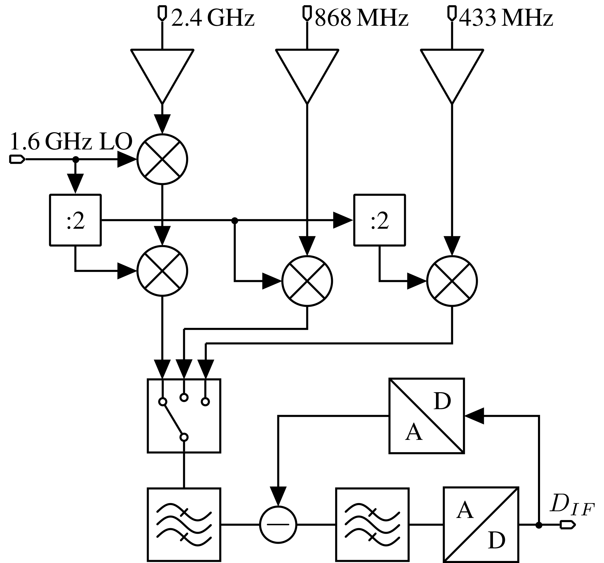
An overview of the relevant parts of the transceiver ASIC is shown as a block diagram of the RX architecture in Fig. 1. The front-end features a sliding-IF mixer for down conversion of the 2.4 GHz band to an intermediate frequency (IF) of 0.5 to 2 MHz depending on the channel bandwidth. The 1.6 GHz local oscillator (LO) signal of the frequency synthesizer is therefore divided by two and used in the second mixer stage. Furthermore the divided LO signal can be connected to the 868 MHz mixers LO input or further divided by two for the 433 MHz mixer. In this way three bands can be supported with only a single phase-locked loop, which is additionally reused for the ASICs transmitter. After down conversion to the desired IF a complex valued quadrature bandpass filter is used for channel selection. Finally, the received signal is converted to the digital domain using a reconfigurable ΔΣM as presented in Saalfeld et al. (2016).
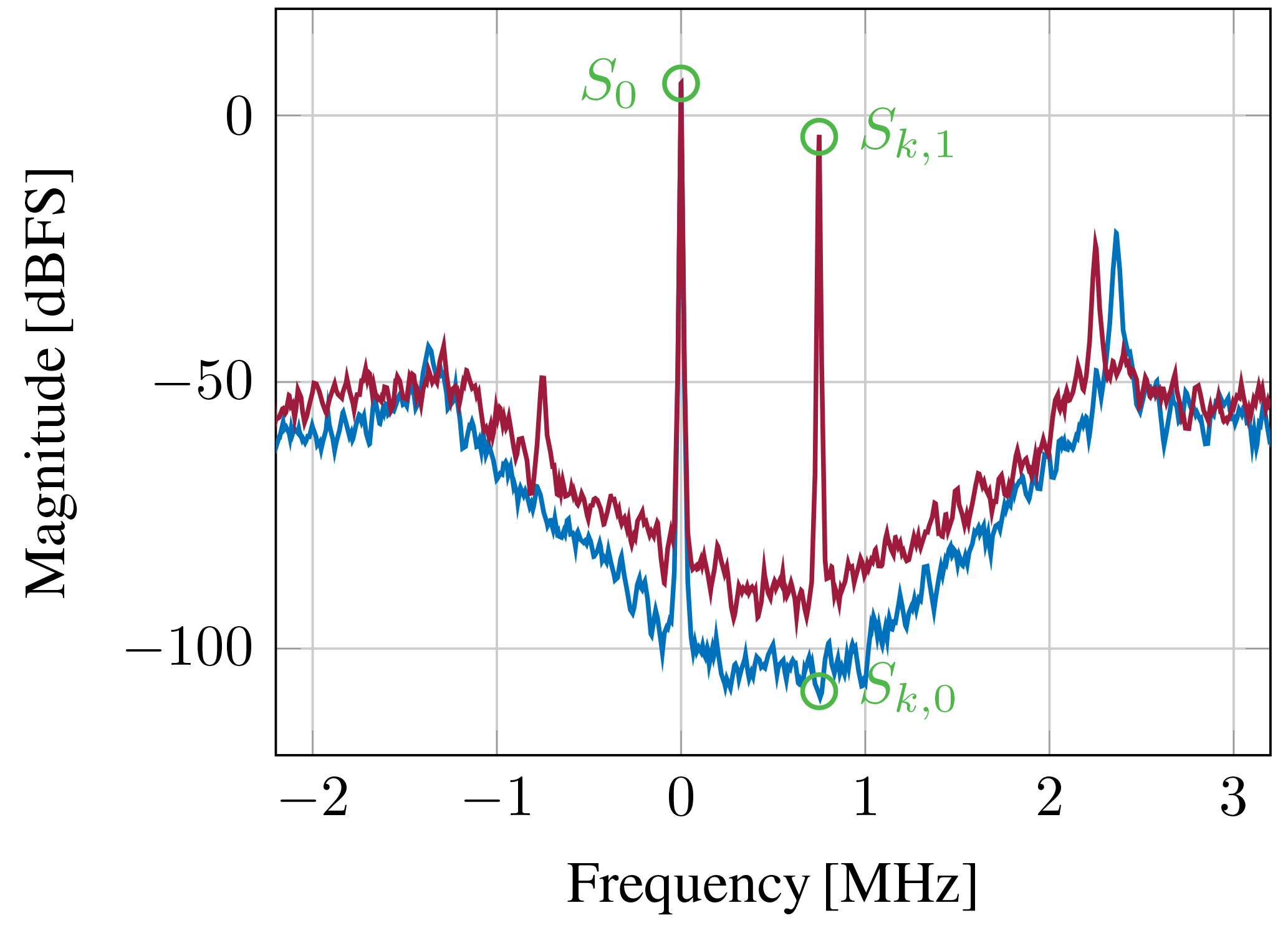
The Fourier transform is a well known and widely used method to analyze a signal in frequency domain. In Fig. 2 the fast Fourier transform (FFT) of simulation data of the single bit mode of the ΔΣM is shown for two scenarios. In one simulation a signal is present at 750 kHz. The corresponding frequency bin is marked as Sk,1. Another simulation has been performed with an input signal amplitude below the quantization noise floor. The corresponding frequency bin has been marked with Sk,0. It can be observed that for both scenarios the DC amplitude S0 is in the same range. In order to determine an RSSI value using a Fourier transform it has to be taken into account that Sk is proportional to the run length. Therefore, S0 can be used to normalize Sk to eliminate this proportionality.
The FFT proves to be an efficient algorithm to calculate the entire frequency spectrum (Ohm and Lüke, 2007). However, more light-weight implementations are available for single frequency bins. Implementing a discrete Fourier transform (DFT) as shown in Eq. (1) for single frequency bins with fixed values of k is a well-fitted solution for signal power detection. Hence, the absolute value of the complex Fourier-coefficient Sk represents the signal power in the kth frequency bin. Furthermore, each bin calculation can be seen as highly selective filtering. Therefore, a narrow band filter for out-of-channel interferer reduction is not necessary.

3.1 Goertzel filter
One approach to the DFT implementation is the Goertzel algorithm. The Goertzel algorithm transfer function is shown in Eq. (2) and is further explained by Oppenheim and Schafer (1999).
Expanding the transfer function with the complex conjugate term, it can be split into an IIR-filter and an FIR-filter as shown in Eq. (3).
Figure 3 shows the corresponding Z-transfer function block diagram. The IIR-filter needs one real multiplication per cycle, while the remaining complex multiplication of the FIR-filter has to be computed only once for every frequency bin.
The resulting algorithm works well with CPUs or DSPs, which have a build-in multiplying unit with sufficient word length, because it reduces the clock cycles required for a complex multiplication to those of a single real multiplication. A VLSI implementation does not benefit in the same way from the reduced multiplication effort, since the complex multiplier has to be implemented in hardware. Furthermore, the real multiplication requires considerable word length, since every error induced by quantization is multiplied in the following cycles. The word length in this case is dominated by the word length of the constant cos-factor, which should be larger than the input word length to achieve the desired resolution.
3.2 Discrete Fourier transform
The DFT can also be directly implemented to compute only a single frequency bin instead of multiple bins as it would be necessary for a spectral range. In Eq. (1) the DFT calculation for the kth frequency bin was already shown. Figure 4 shows the corresponding Z-transform block diagram. It consists of a multiplication stage and an integrator. In contrast to the Goertzel algorithm a time dependency introduced by the index n exists for fixed values of the selected bin k and the spectral resolution N.
However, the DFT works well with ΔΣM because the high resolution is achieved with oversampling and noise shaping instead of a high number of bits. The higher frequency barely has an effect on the VLSI implementation, while a higher number of bits would directly increase the physical size of the multiplier. Utilizing the single bit data stream of the ΔΣM allows to minimize the size of the multiplier in the input path. Furthermore, the down conversion of the received signal from IF to DC is typically performed by the demodulator as shown by Y. Zhang et al. (2013). Hence, the down conversion multiplication with e−jω should already be implemented by the DSP.

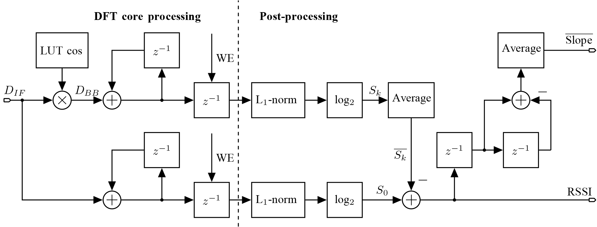
The presented architecture, depicted in Fig. 5, uses the single bit ΔΣM samples. Since the values represent ±1 the complex multiplier can be implemented as sign selection. A base 2 logarithm unit is included to allow linear mapping between the calculated RSSI and the signal power in dBm. Additionally, the common mode coefficient S0 is calculated, as shown in Eq. (4).
The absolute value of the relevant frequency bin, , is normalized to to have an RSSI value independent of the run length.
As seen in Eq. (5) the normalization is realized by subtracting the logarithmic values, eliminating the need for a divider unit. Continuous calculation allows variable computation time, running as long as necessary, but as short as possible.
4.1 DFT core processing
The calculation of the DFT is shown as the core processing part in the left section in Fig. 5. As stated in Sect. 3.2 the index value n of the complex e−jω multiplication shown in Fig. 4 changes with every cycle. Therefore, a lookup table (LUT) has to be introduced. If the computation runs continuously, then the sample count N in Eq. (1) is time variant. Furthermore, the resulting spectral resolution and therefore the width of the detected frequency bin is dependent on N as well. Higher N result in narrower frequency bins and thus increasing the signal to noise ratio (SNR) in this specific bin. During computation the observed bin is fixed in regard to the absolute frequency and is defined by the factor which is therefore constant and independent over the run length. Hence the computation can run continuously and does not necessarily need a fixed duration. This increases the resolution, allowing to detect signals with low power levels which would otherwise have been indistinguishable from the noise. Consequently, longer computation time enables the detection of small signals.
Regarding the LUT values the exponential term in Eq. (1) can be replaced using Euler's formula. As seen in Eq. (6) a cosine value as well as a cosine shifted by a quarter period are required.
The cosine argument is periodic at , where the largest N in the presented system is set by the maximum ΔΣM clock frequency fs=96 MHz. The smallest necessary k is set by the lowest IF fIF=0.5 MHz and is the index of the relevant frequency bins for RSSI detection. This results in a cosine LUT length of for a full period. However, storing a quarter period is sufficient to reconstruct the entire cosine, reducing the size of the LUT to 48 entries. Reconstruction is done by either negating the LUT value or reversing the access. The need to access the values in reverse as well as in regular order simultaneously requires individual multiplexer-trees for the sine and cosine values.
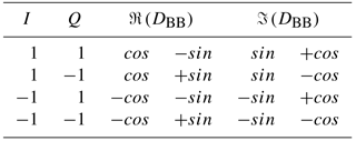
The input is a complex value defined by the ΔΣM output values and has to be interpreted as . The complex multiplier at the input is split into four real multiplications, where sin and cos represent the sine and cosine term in Eq. (6). The resulting signal is interpreted as shown in Eq. (7). The sign selection of cos and sin values depending on the input signal DIF is shown in Table 1.
Table 1LUT signal selection for single bit complex multiplication.
If the input from the ΔΣM is negative and the index n requires the LUT value to be inverted, the resulting value will be positive. Therefore, the inversion is controlled by the exclusive disjunction and realized within the following accumulator. Reusing the accumulator adder requires no additional summation stage for the two's-complement. This accumulator consists of an adder and a register to store the current complex Fourier coefficient. An additional pipeline register delays further processing of the Fourier coefficient until at least one full period of the exponential term in Eq. (1) is calculated. Consequently, calculations with incomplete coefficients are prevented.
For the detection of the DC value the coefficient k in Eq. (6) is set to k=0 as shown in Eq. (4). Therefore, the multiplication is not necessary and only an accumulation stage is needed.
4.2 Post-processing
The L1-norm is a sufficient method to be used in an RSSI detection. Shown in Eq. (8) is the result of an L1-norm of the Sk signal. The absolute value is generated by checking the sign and, if necessary, negating ℜ or ℑ of Sk during the following summation.
For logarithm calculation the value is, as discussed by Mansour et al. (2014), divided into mantissa and exponent. As shown in Fig. 6 the logarithmic value can be expressed as:
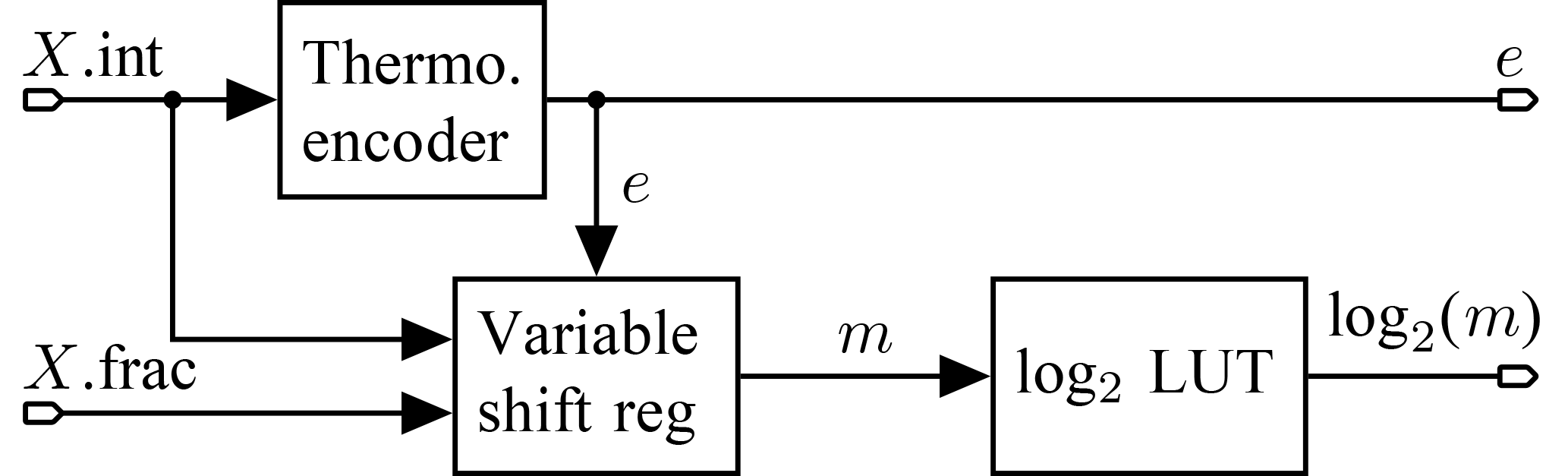
The exponent e is calculated using a thermometer encoder, while the mantissa m is generated by shifting the original value X by e bits. This is performed by a variable shift register, which requires one clock cycle per shift. The mantissa is then fed to a LUT with a size of 32 values that maps m to log 2(m). By using a fixed point format the exponent and the logarithmic mantissa can be concatenated, yielding the final logarithmic value. Small variances between concurrent log 2(Sk) values are attenuated, using a moving average filter with a length of four. A signed subtracter finally calculates the RSSI value.
The difference of the last two RSSI values is evaluated using an approximate derivative of the RSSI signal. Once the RSSI has converged, the absolute value of this difference drops below a threshold and the RSSI calculation can be stopped. Furthermore, the current slope is given out alongside the RSSI, giving a factor for RSSI quality estimation.
Luo et al. (2013)Huang et al. (2000)Table 2Comparison of the proposed digital algorithm with analog limiting amplifier based implementations.
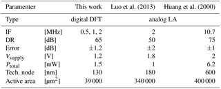
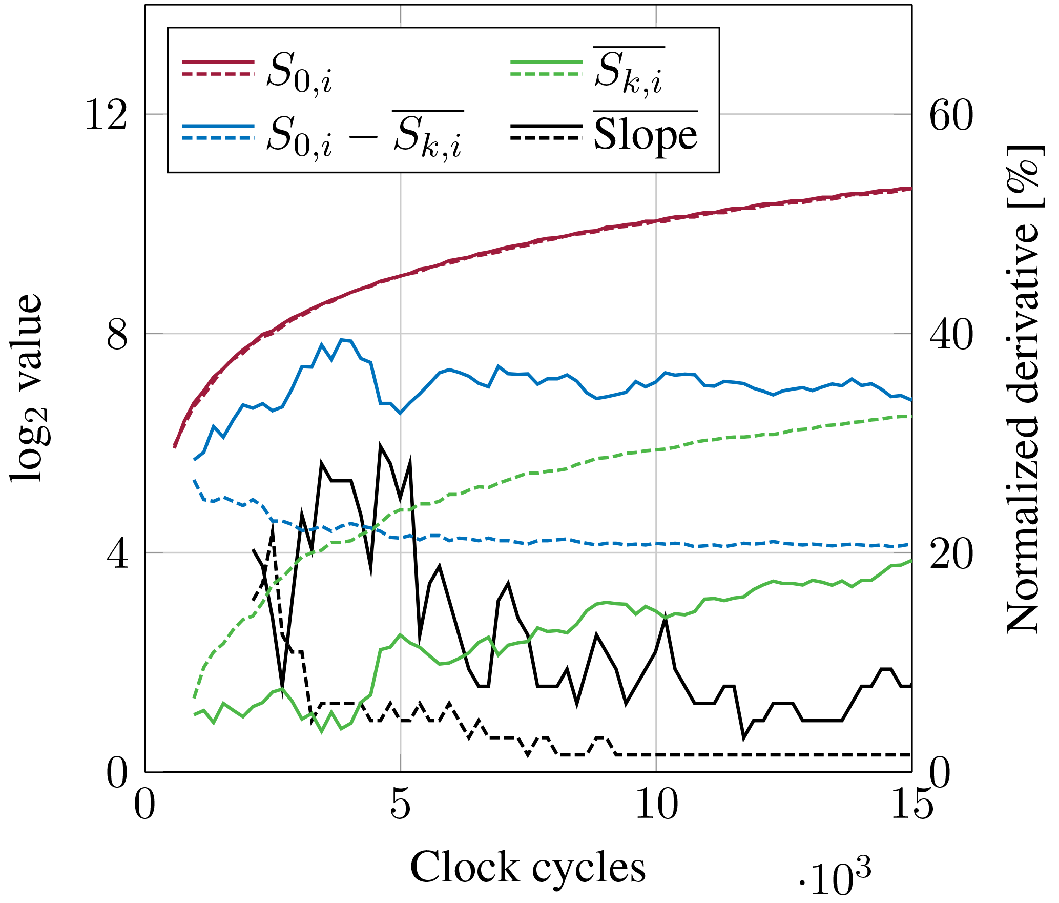
Figure 7Development of the RSSI during simulation over run time for an input power of −70 dBm (solid) and −50 dBm (dashed).
Figure 7 shows the RSSI value, the individual frequency bins as well as the derivation of the RSSI, called Slope. Using the existing ASIC and an FPGA, single bit ΔΣM samples have been recorded and used for simulations. A high language description of the hardware was used for the simulations, ensuring early verification of the algorithms functionality. Figure 7 depicts the development of the RSSI (), the DC value S0 and the Sk value as well as the slope shown in percent. The data is exemplary shown for −70 and −50 dBm input power. It can be seen that the DC value S0 is equal for both input powers, while settles to higher values with higher input power. Furthermore, the decreased settling time for increased input power values can be observed.
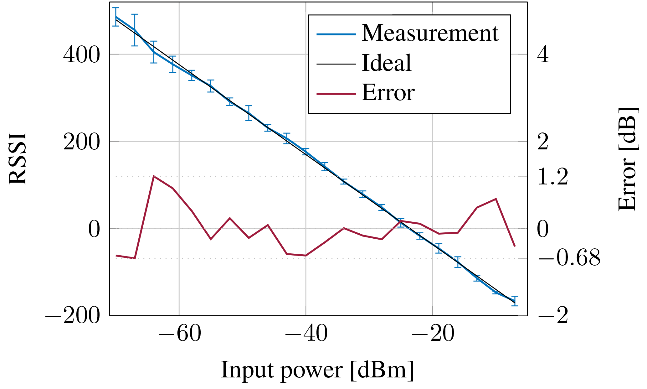
The design functionality has also been verified in measurements using VHDL code synthesized on a Xilinx Virtex 5 board. The design was tested using the existing transceiver ASIC in receive operation as presented in Sect. 2. The RF input signals were supplied by a signal generator. Figure 8 shows the RSSI measurement with a step size of 3 dB. Furthermore, the standard deviation over 10 runs is shown for each measured input signal power.
Additionally, the error of the measured RSSI towards an ideal regression is shown in dB with respect to the input power. It can be seen that for all input power measurements the RSSI error stays below 1.2 dB while the standard deviation increases for smaller input signals due to the decreased SNR.
In order to integrate the ED within the transceiver ASIC a synthesis for a 130 nm RF CMOS technology has been evaluated. The measurement results and worst case synthesis report for power and area consumption are used for a comparison to analog LAs in Table 2. The DFT based implementation shows a decent power consumption Ptotal=1.5 mW during calculation with a small area of 39 000 µm2. It has to be pointed out that for the analog LA based implementations the LA is an essential system block of the used RX architecture unlike in a low-IF architecture. Furthermore, LA would need a separate ADC in order to provide a digital RSSI value. Additionally, the integration into a transceiver ASIC would allow the reuse of the down conversion to BB during demodulation reducing the power consumption of the proposed implementation by 6 %. In regards to the DR and error the DFT based digital implementation shows an adequate performance.
A receiver signal strength detection algorithm based on a discrete Fourier transform algorithm has been presented. It evaluates the single bit output data stream of a ΔΣ modulator without previous signal manipulation like digital filtering. Furthermore, the ED has been verified in measurements using a custom ASIC with a low-IF RX. It features a DR of 65 dB with an error of less than 1.2 dB and provides an input power dependent run time by evaluating the derivative of the RSSI signal. The synthesized hardware implementation for a 130 nm RF CMOS technology showed a small area of 39 000 µm2 and power consumption of less than 1.5 mW. Consequently, an efficient DFT based implementation for ED has been shown which can directly be used as a low effort solution for RSSI calculation in low-IF architectures with ΔΣM.
The raw data for simulation, simulation output data and measurement results are available at Zenodo (https://doi.org/10.5281/zenodo.1260387; Saalfeld and Piwczyk, 2018).
The authors declare that they have no conflict of interest.
This article is part of the special issue “Kleinheubacher Berichte 2017”. It is a result of the Kleinheubacher Tagung 2017, Miltenberg, Germany, 25–27 September 2017.
The authors acknowledge the financial support by the German Federal Ministry
of Education and Research (FKZ 16 ESEO154) and the Electronic Components and
Systems for European Leadership Joint Undertaking under grant agreement No.
737434.
Edited by: Jens Anders
Reviewed by: two anonymous referees
Atmel AT86RF233: Low Power, 2.4 GHz Transceiver for ZigBee, RF4CE, IEEE 802.15.4, 6LoWPAN, and ISM Applications, Datasheet, Atmel, rev. 8315E–MCU Wireless–07/14, available at: http://ww1.microchip.com/downloads/en/DeviceDoc/Atmel-8351-MCU_Wireless-AT86RF233_Datasheet.pdf (last access: 20 January 2018), 2014. a
Ho, C. Y., Chan, W. S., Lin, Y. Y., and Lin, T. H.: A Quadrature Bandpass Continuous-Time Delta-Sigma Modulator for a Tri-Mode GSM-EDGE/UMTS/DVB-T Receiver, IEEE J. Solid-St. Circ., 46, 2571–2582, https://doi.org/10.1109/JSSC.2011.2164026, 2011. a
Huang, P.-C., Chen, Y.-H., and Wang, C.-K.: A 2-V 10.7-MHz CMOS Limiting Amplifier/RSSI, IEEE J. Solid-St. Circ., 35, 1474–1480, https://doi.org/10.1109/4.871325, 2000. a, b
IEEE 802.15.4: Standard for Low-Rate Wireless Networks, IEEE Std. 802.15.4™-2015, New York, USA, https://doi.org/10.1109/IEEESTD.2016.7460875, 2016. a, b, c
Luo, R., Bai, X., Diao, S., and Lin, F.: A 1mW CMOS Limiting Amplifier and RSSI for ZigBee™Applications, in: Proceedings of the IEEE International Wireless Symposium, 1–4, https://doi.org/10.1109/IEEE-IWS.2013.6616734, 2013. a
Mansour, A. M., El-Sawy, A. M., Aziz, M. S., and Sayed, A. T.: A New Hardware Implementation of Base 2 Logarithm for FPGA, International Journal of Signal Processing Systems, 3, 177–182, https://doi.org/10.12720/ijsps.3.2.177-182, 2015. a
Ohm, J.-R. and Lüke, H. D.: Signalübertragung: Grundlagen der digitalen und analogen Nachrichtenübertragungssysteme, Springer, Berlin, Heidelberg, 94–97, https://doi.org/10.1007/978-3-540-69258-4, 2007. a
Oppenheim, A. V. and Schafer, R. W.: Discrete-Time Signal Processing, 2nd Edn., Prentice Hall, Upper Saddle River, New Jersey, 1989. a
Raja, M. K., Chen, X., Lei, Y. D., Bin, Z., Yeung, B. C., and Xiaojun, Y.: A 18 mW Tx, 22 mW Rx Transceiver for 2.45 GHz IEEE 802.15.4 WPAN in 0.18-µm CMOS, IEEE Asian Solid Sta., 1–4, https://doi.org/10.1109/ASSCC.2010.5716552, 2010. a
Saalfeld, T. and Piwczyk, T.: Measurement Results of Single-Bit Sigma-Delta Modulator and Simulation Data for DFT Based RSSI Calculation, https://doi.org/10.5281/zenodo.1260387, 2018. a
Saalfeld, T., Atac, A., Liao, L., Wunderlich, R., and Heinen, S.: A 2.3 mW Quadrature Bandpass Continuous-Time ΔΣ Modulator with Reconfigurable Quantizer, in: Proceedings of the 12th Conference on PhD Research in Microelectronics and Electronics, https://doi.org/10.1109/PRIME.2016.7519526, 2016. a
Zhang, L., Jiang, H., Wei, J., Dong, J., Li, F., Li, W., Gao, J., Cui, J., Chi, B., Zhang, C., and Wang, Z.: A Reconfigurable Sliding-IF Transceiver for 400 MHz/2.4 GHz IEEE 802.15.6/ZigBee WBAN Hubs With Only 21 % Tuning Range VCO, IEEE J. Solid-St. Circ., 48, 2705–2716, https://doi.org/10.1109/JSSC.2013.2274893, 2013. a
Zhang, Y., Wang, Y., Wunderlich, R., and Heinen, S.: A Novel Low-Effort Demodulator for Low Power Short Range Wireless Transceivers, IEEE T. Circuits.-I., 60, 2521–2532, https://doi.org/10.1109/TCSI.2013.2246205, 2013. a
Zolfaghari, A., Said, M. E., Youssef, M., Zhang, G., Liu, T. T., Cattivelli, F., Syllaios, Y. I., Khan, F., Fang, F. Q., Wang, J., Li, K. Y. J., Liao, F. H. F., Jin, D. S., Roussel, V., Lee, D. U., and Hameed, F. M.: A Multi-Mode WPAN (Bluetooth, BLE, IEEE 802.15.4) SoC for Low-Power and IoT Applications, in: Digest of Technical Papers of the 2017 Symposium on VLSI Circuits, C74–C75, https://doi.org/10.23919/VLSIC.2017.8008554, 2017. a