 | 19 Sep 2019
Analysis of the frequency conversion of spurious tones in frequency dividers and development of an event-driven model for system simulations
Christoph Beyerstedt
Jonas Meier
Fabian Speicher
Ralf Wunderlich
Stefan Heinen
This paper presents a frequency domain analysis of spurious tones in frequency dividers. The results of the analysis are used to develop an event-driven model for system simulations which work entirely in the frequency domain. The proposed approach is able to provide a fast and accurate model in a SystemVerilog/C++ environment which takes the frequency conversion effects of the spurious tones into account. A virtual prototype which includes the model was simulated and due to the fast simulation speed it was possible to determine the influence of spurious tones on the bit error rate in a complex receive scenario.
- Article
(1855 KB) - Full-text XML
- BibTeX
- EndNote


The trend in modern system-on-chips (SoCs) is going towards integration of many different subsystems on a single die. Especially for integrated RF-transceivers it brings a challenge due to the complex modulation schemes needed for high data rates and flexibility of the system. On the one hand, a high sensitivity for the receivers and a pure spectral mask of the transmitters are crucial, on the other hand, due to the integration of multiple transceive paths with control logic and digital signal processing on one chip, many sources of digital supply noise exist which can couple in sensitive analog blocks and harm the performance of a transceiver (Hung and Muhammad, 2010). One component, which is crucial for every transceive system is the high frequency clock generation block used for up- and downconversion of the baseband signals. Usually a phase locked loop (PLL) is used for this purpose (Elsayed et al., 2013). Ideally the PLL output is a perfect sine signal but in reality the output signal contains other unwanted frequency components due to switching events inside the blocks and coupling of noise in the components of the PLL (Gao et al., 2010; Lee et al., 2001; Saeed, 2012). In many transceiver architectures the PLL output signal is not directly used but first divided by a frequency divider (FD) before being fed to a mixer. This is advantageous because the pulling of the output power amplifier (PA) on the oscillator can be attenuated if the PA output frequency is not the same as the VCO frequency (Razavi, 1999). Furthermore, in complex valued receivers, a frequency divider can be used to generate two local oscillator (LO) signals shifted by 90∘ for an IQ mixer (Bardin and Weinreb, 2008).
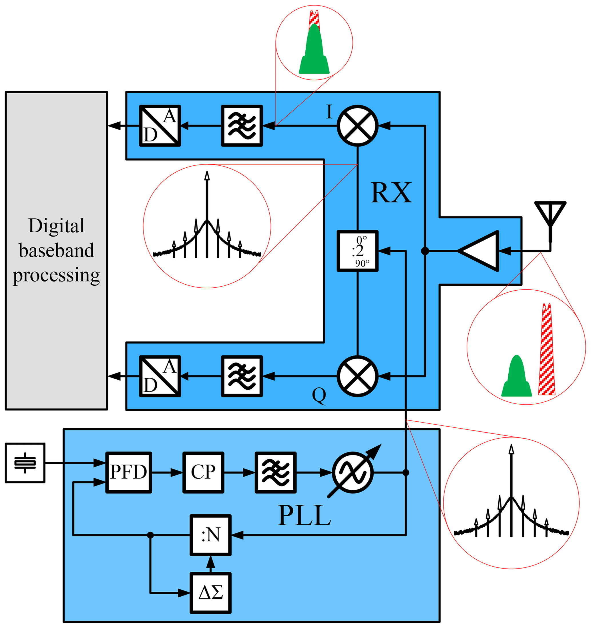
For frequency planing of the transceivers it is crucial to know where the unwanted frequency components of the local oscillator are converted to by the frequency divider. Figure 1 shows a scenario of an IQ receiver with a small wanted signal in green and a large blocker depicted as red hatched signal. The PLL output contains the main tone and several spurious signals. The spurs are converted by the frequency divider in such way, that one spur mixes the input blocker directly into baseband. The downconverted input signal is now disturbed by the blocker signal, the signal-to-noise ratio (SNR) is lowered and the bit error rate (BER) degrades. This can only be avoided by careful frequency planning and therefore it is important to know, where the spurs are located at the output of the frequency divider. Due to the complexity of modern transceive systems, it is impossible to do this completely by hand. Therefore, a fast and accurate model is needed which supports the simulation of a complete SoC to cover all influences from other parts of the chip. To achieve a reasonable degree of simulation speed, the use of an event-driven simulator is required (Chen, 2009). For further speed-up, the frequency divider model should not work in the time domain but uses a spectral representation of the signal (see Sect. 3).
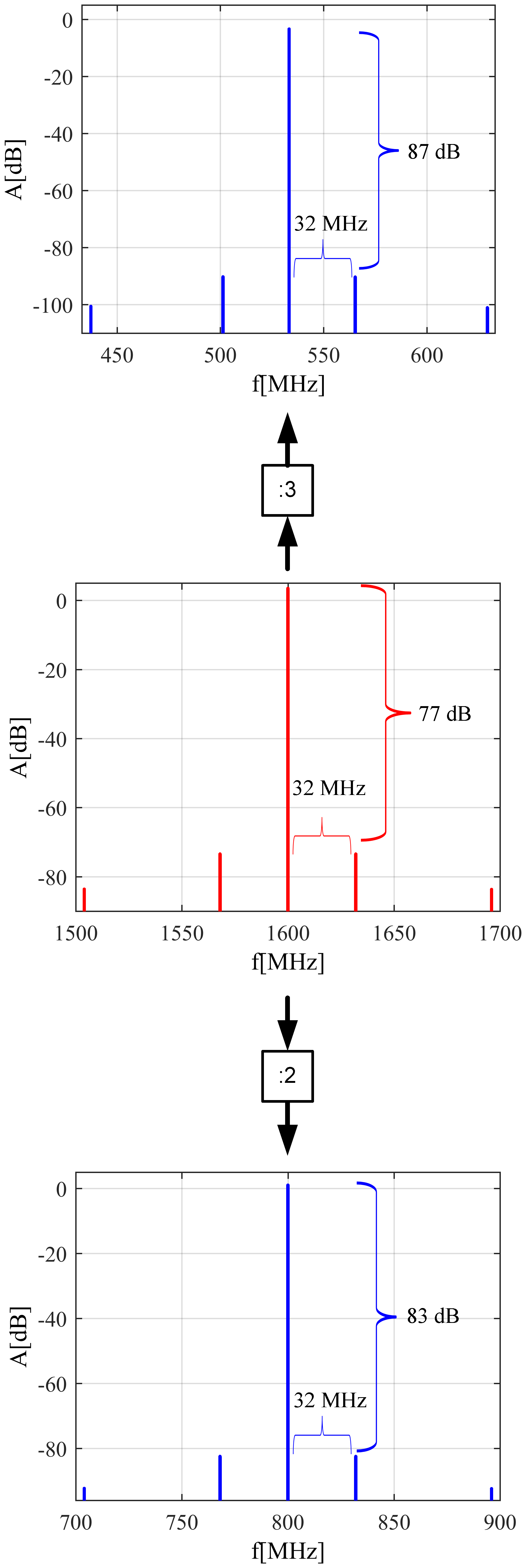
Due to the fact that frequency dividers are strongly nonlinear and have a memory, the conversion of the spurious tones are not straightforward as one would expect. Naively one would say that the frequency of every spectral component just gets divided by the divider factor but frankly this is not the case. A circuit simulation of a frequency divider by two and a divider by three showed, that only the frequency of the main (largest) tone is divided by the divider factor. The spurious component at the offset frequency (foff) of 32 MHz can be found in the output signal at the same offset but with reduced amplitude (see Fig. 2).
A deeper look in the mathematics of spurs and frequency dividers can explain this behavior. The input signal with spurious tones of a FD is a quasiperiodic signal with constant amplitude. Simplified, these class of signals can be described as follows:
with:
Under the assumption that the amplitudes asp,i are small, the amplitude of the spurious tones can be derived from Eq. (1) by splitting the equation with the trigonometric theorems: As can be seen the spurs originate in the periodic changes in the phase of the clock signal.
with:
The output signal of a frequency divider can be easily derived from the FD input signal as described in Eq. (1). The FD counts the input rising or falling edges and toggles its output depending on the divider factor N. When looking on the phase of the input and output signal, this behavior can be described by dividing the input phase by N (Egan, 1990). Thus, the output signal of the FD can be described as follows:
By splitting Eq. (3) the same way as Eq. (1), the output spectrum of the FD can be calculated.
with:
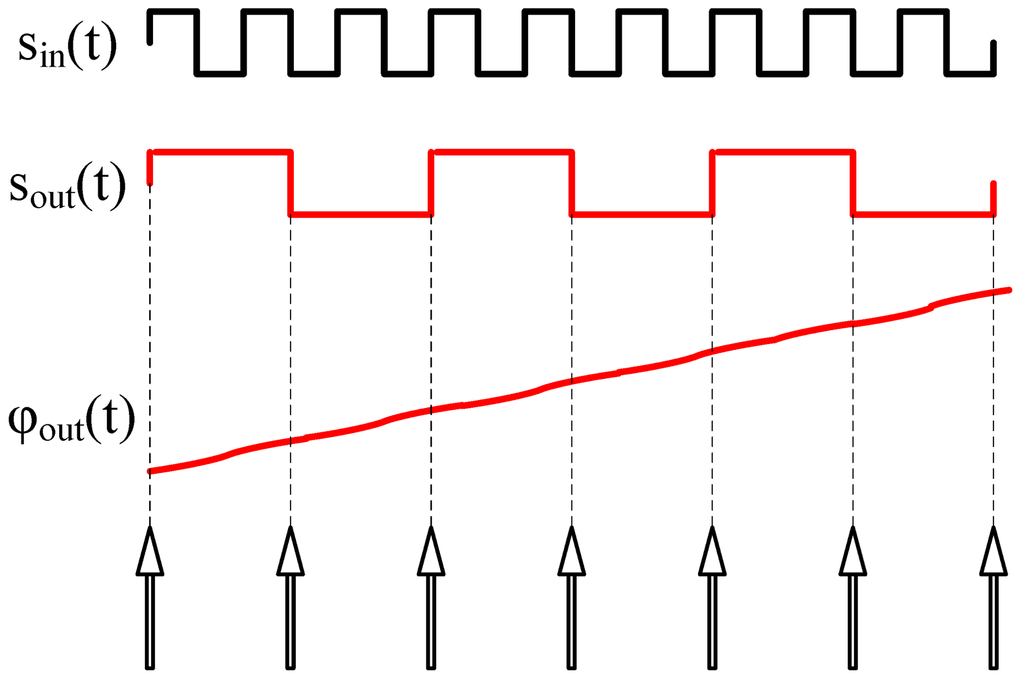
When comparing the FD input spectrum (Eq. 2) with the output spectrum (Eq. 4), it can be seen on the first sight, that the spur offset frequencies ωsp,i stay the same and are not influenced by the divider factor, but the amplitude of the spurs are scaled with . For small offset frequencies compared to the output frequency of the FD, this approximation of the FD behavior is good enough. But for large offset frequencies another effect of frequency dividers has to be considered. The switching of the output port of the FD is dominated by the largest tone of the output signal. Furthermore the influence of the spurious tones can only be observed at the transitions of the output signal. Thus, as a good approximation, it can be said that the spurious output tones get sampled by the positive and negative edges of the output main signal component of the FD (Apostolidou et al., 2008). Figure 3 gives shows graphically the sampling of the phase by the output main tone. A FD with a divider ratio of 8 and a output duty cycle of 0.5 was simulated on transistor level. The input signal is composed of a large tone at 1.6 GHz and a spur at 2.038 GHz. At the output there are not only the downconverted spurious output tones but also replica of them in the distance of 400 MHz due to the sampling of the spurs by the edges of the 200 MHz output main tone (Apostolidou et al., 2008). As one can see in Fig. 4 spurious tones with offset frequencies larger than twice the output frequency (438 MHz) can be folded very close to the output main tone and lead to unexpected spurs (38 MHz).

For understanding the modeling approach of the FD, a small detour to the signal description in the used simulation environment is necessary. The spectral signal description is similar to the baseband equivalent signal description, which is a widely used approach to speed up simulations of event-driven real number models of RF systems. It is based on the fact that every modulated RF signal can be represented as:
where fRF is the carrier frequency and I and Q describes the baseband information (Chen, 2009). The complete information is in I, Q and the carrier frequency and so it is sufficient to pass the baseband equivalent signal
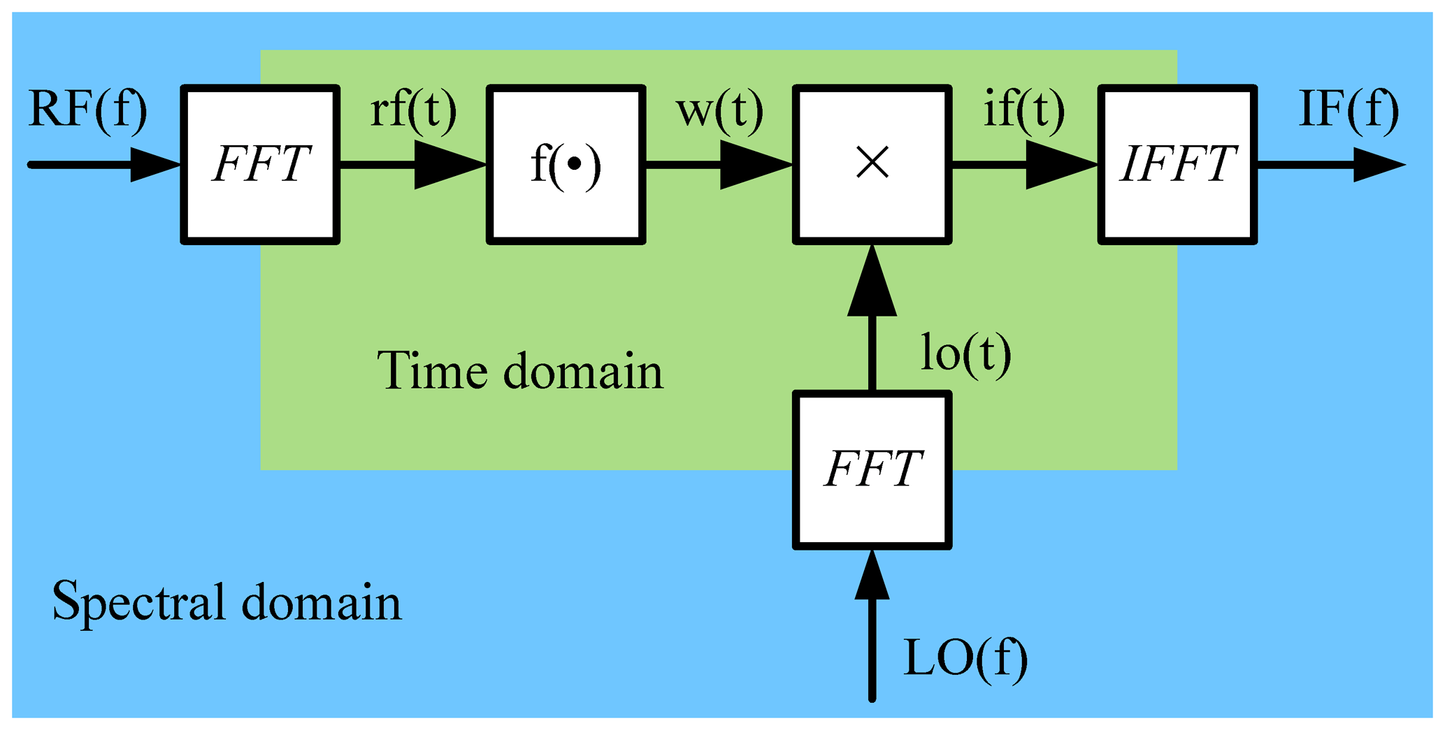
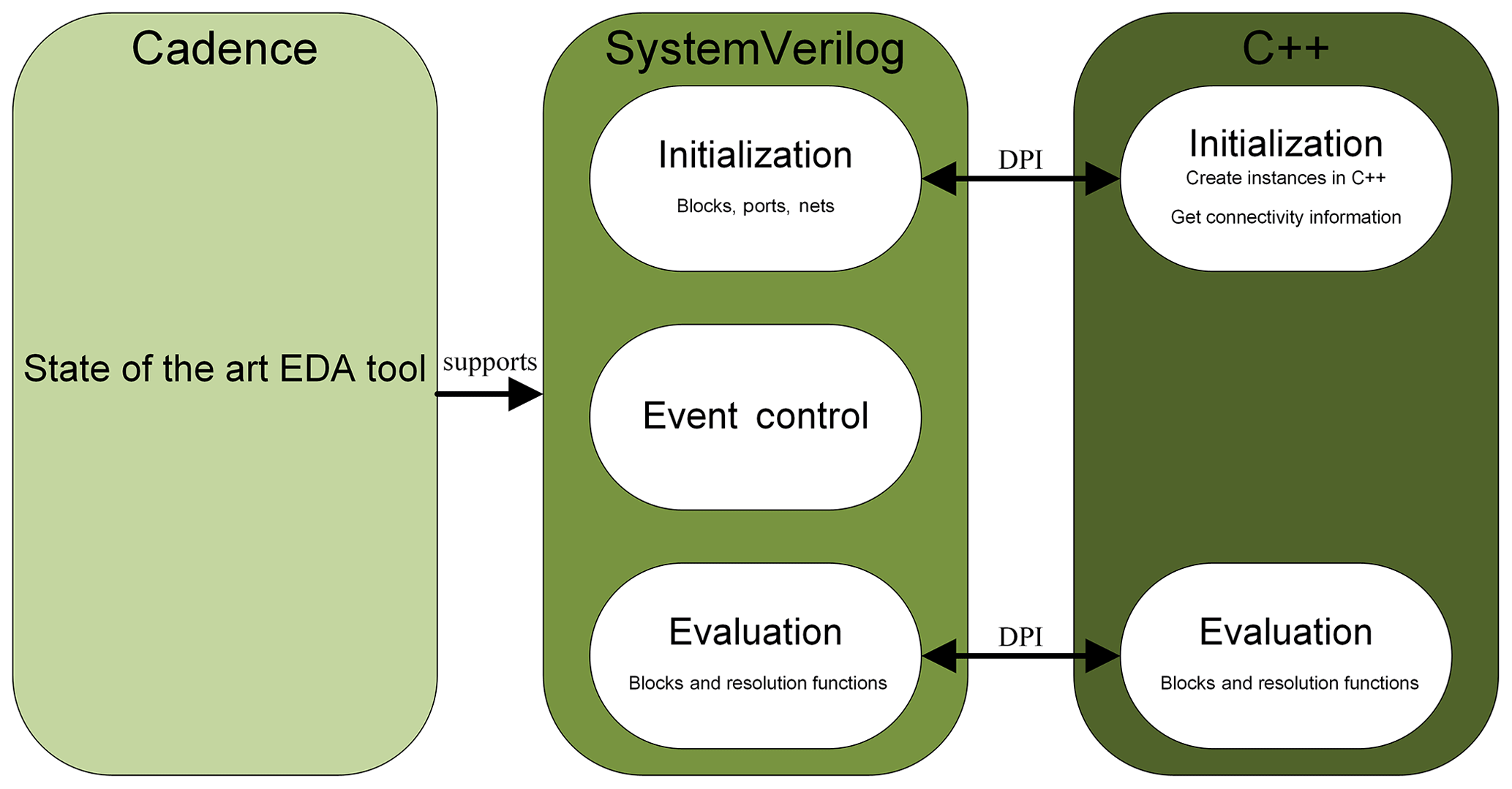
and the center frequency fRF between the models to recover the full signal. Since the high frequent oscillation is suppressed, significantly fewer events are generated and therefore the simulation speed increases (Chen, 2009). While this signal description is sufficient for systems with one RF signal, it fails when multiple frequency components appears in the signal as it is the case when describing a spurious clock signal in frequency domain. A solution to this problem is to allow an array of baseband equivalent signal for every carrier frequency in the signal. To capture nonlinear effects it is also beneficial to store harmonics and possible intermodulation products of the frequency components. This is possible by using a multidimensional vector space (Speicher et al., 2018). Furthermore switching between spectral and time domain can be easily done by using multidimensional fourier transforms. This is advantageous when modeling nonlinearities or mixing processes. Like in a harmonic balance simulator (Kundert, 1999), the signal is first transformed in time domain, the nonlinearity is applied and the signal is transformed back in the spectral domain (see Fig. 5). The spectral signal is implemented in a SystemVerilog/C++ modeling framework (see Fig. 6). The advantage of this approach is, that the hardware description language SystemVerilog (SV) can be natively used in the state-of-the-art Cadence EDA environment. A SV model can simply be added to the designed blocks of the system. The structural information of the complete design stays the same when using the models instead of the transistor level implementation and the netlist can be reused. Also the event handling can be easily done in SV and does not have to be implemented in another programming language. The direct programming interface (DPI) of SV gives the possibility to access and use functionality of precompiled code of languages like C++. All necessary calculations in the models are executed in C++ and benefit from the powerful algorithms and data containers already available there. For the switching between the time and the spectral domain, the powerful FFTW library (Frigo and Johnson, 2005) is used, which can efficiently execute multidimensional fourier transforms. A more detailed description of the spectral signal can be found in Speicher et al. (2018).
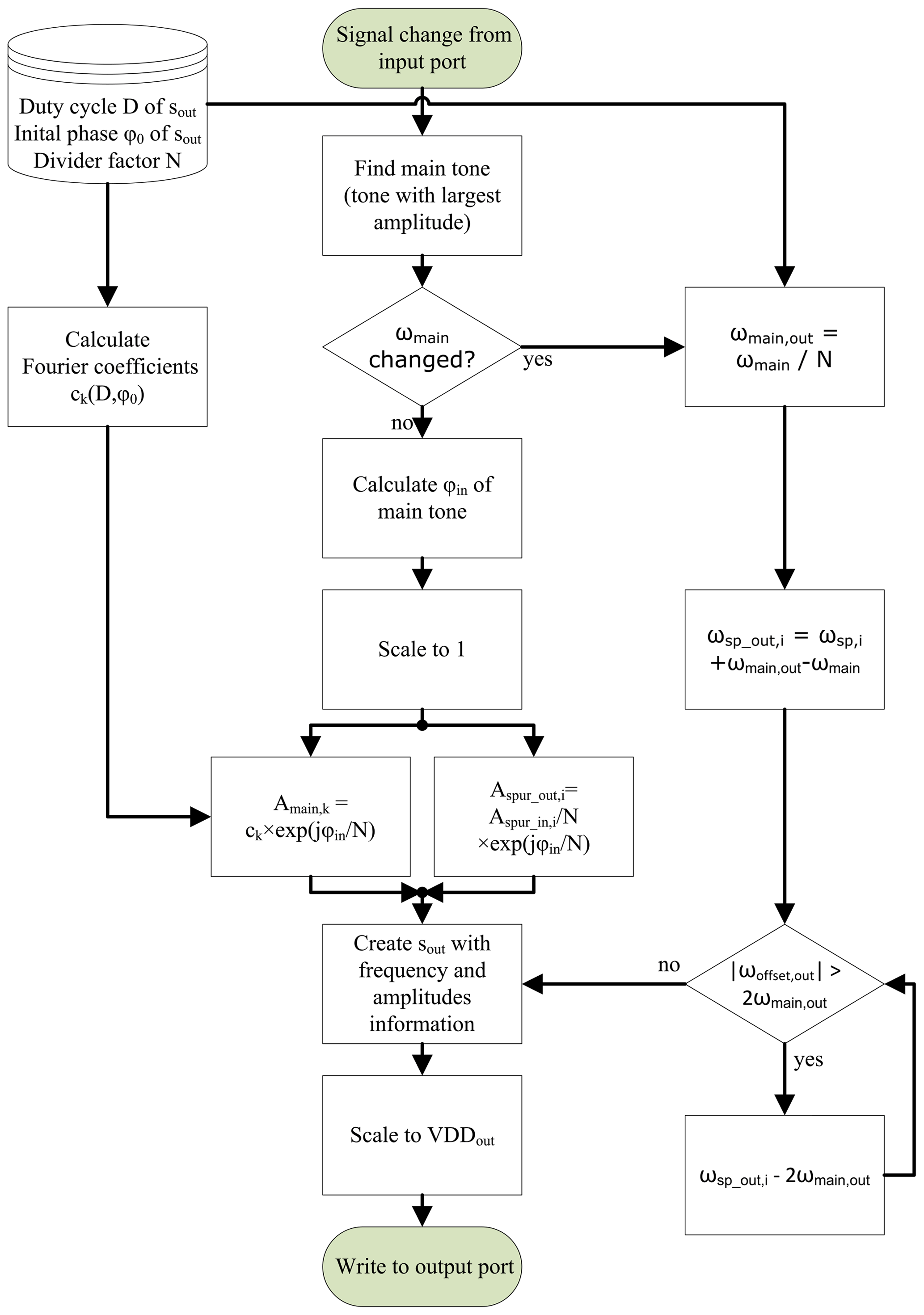
As mentioned in Sect. 1, the aim of this work is to develop a fast FD model for event-driven simulations. A simple approach for a frequency divider model is to count the transitions of the input signal and toggle the output signal after N rising or falling edges (Wang et al., 2009). But this approach has several drawbacks in combination with the spectral signal description. First of all for a signal with a high frequency many events are generated which slows down the entire simulation. For example for a 2 GHz signal, at least 4 billion (2 events per period for rising and falling edges) events per second will be generated. Furthermore when having multiple tones with inconsummerate frequencies in a signal the calculation of one period is hard and therefore calculating the fourier transform looking for the period of the input signal and calculating the output frequencies out of that is a bad idea. To the authors knowledge there are no suitable event-driven frequency divider models which supports spectral in- and output signals. For the development of the FD model which works with spectral signals, the results from Sect. 2 are used. Figure 7 describes the model of the frequency divider in a flow chart. After an input event, the largest tone is searched in the spectral signal. After that, it is checked whether the main tone has changed or not and in case of a new dominant fundamental, the output frequency components are recalculated. To keep the spectral output signal in a reasonable size, only the aliasing component of the spurs which are closest to the output main tone and therefore for the most scenarios most critical are attached in the output spectrum. The amplitudes of the output spectrum are calculated separately, depending on whether it is the amplitude of the main tone or it is a spur amplitude. Furthermore, the current, time dependent phase of the input main tone is determined. It is coded in the I and Q part of the main tones amplitude. For a fast phase calculation, the current input frequency deviation is calculated by differentiation of the input phase ϕin of the main tone.
The output frequency deviation for the main tone can be calculated by dividing the input frequency by N. The output phase can be calculated from the output frequency and included in the calculation of the output amplitudes (see Eq. 4).
Due to the fact that the input and the output level of the signals might be different, a scaling before and after the amplitude calculation is done.
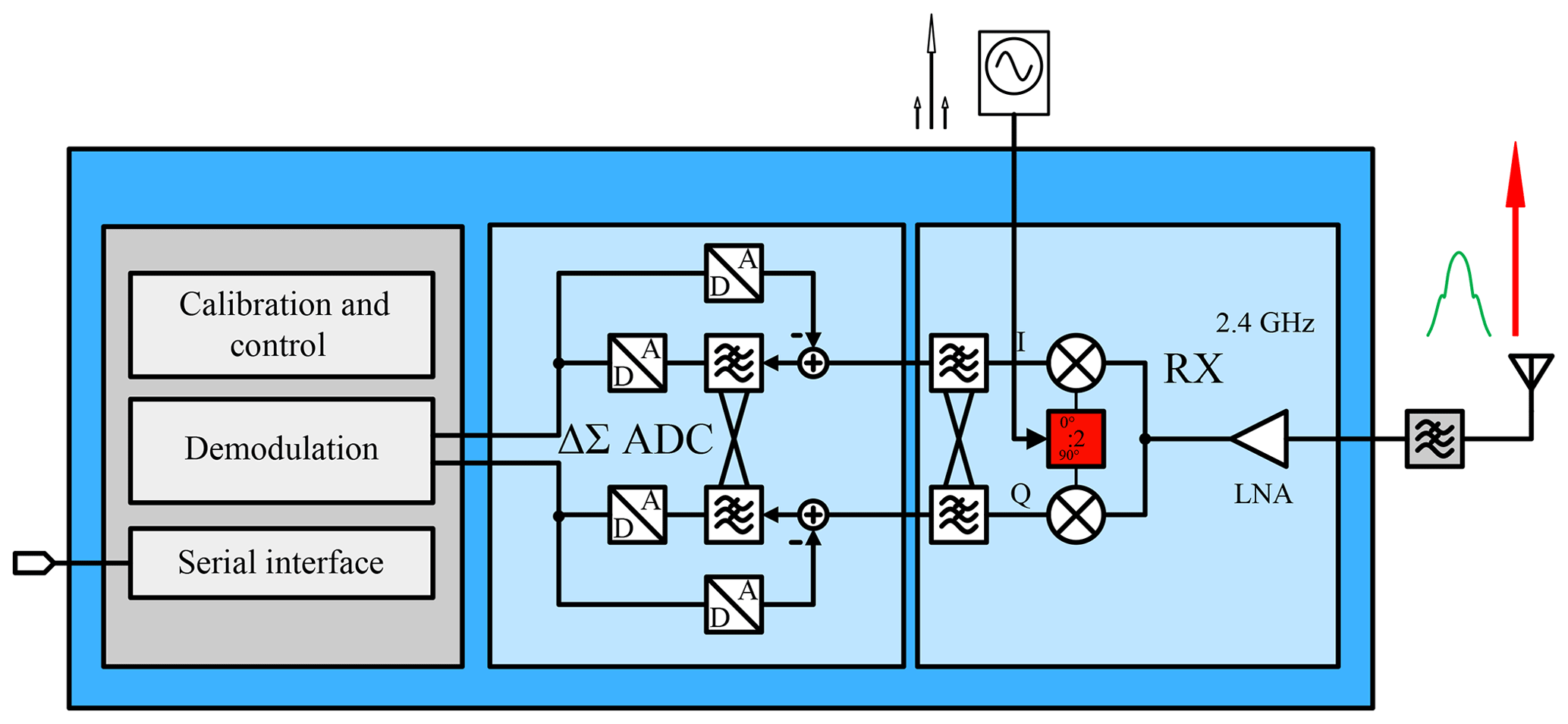
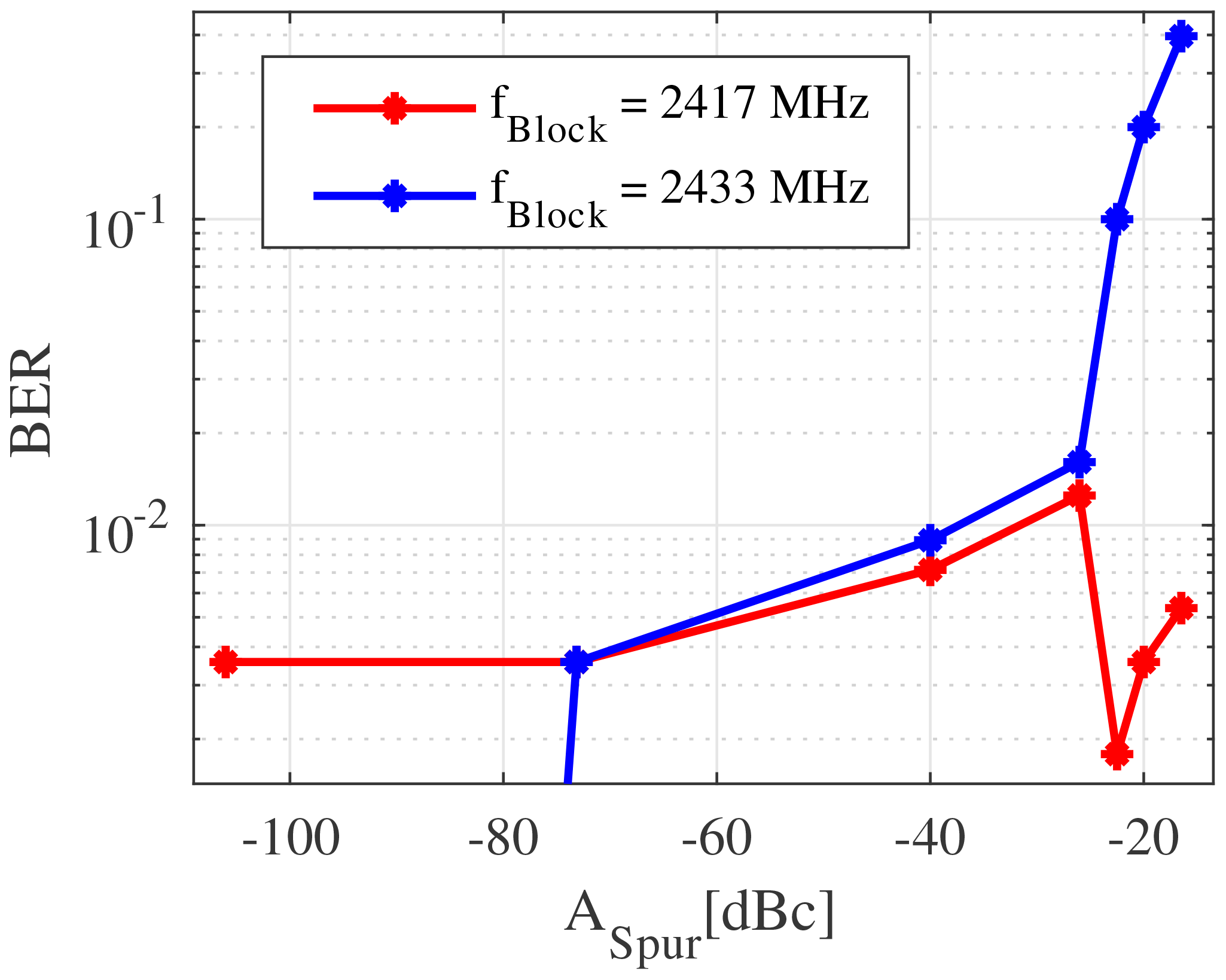
The frequency divider model was used in a virtual prototype of an integrated 2.4 GHz low-if receiver shown in Fig. 8. It consists of an LNA, an IQ mixer driven by a frequency divider, which generates the I and Q LO signals, a polyphase channel filter and a ΔΣ-ADC. The output signal of the ADC is fed to a digital demodulator. Furthermore, the digital part contains calibration and control routines and a serial interface to control the chip. Bit error rate simulations of the complete system were done using SystemVerilog/C++ models for the analog components of the receiver. The LO signal was assumed to be at 4.8 GHz with spurs at an offset frequency of ±32 MHz. Two different blocker scenarios were examined. In the first case, a blocker at 16 MHz offset from the input center frequency of 2.401 GHz was added to the GFSK input signal. The second simulation was done with a blocker at 32 MHz offset frequency. Furthermore the amplitude of the LO spurs were stepwise increased. The BER for both test cases is shown in Fig. 9. As can be seen the BER is greatly affected by the spur amplitude when the mixing product of the spur and the blocker falls into the baseband. Otherwise the BER varies only little over the spur amplitude. 560 transmitted bits were simulated per spur level. The simulation speed can be calculated to 10.64 µs simulated time per second. For speed comparison a reference transistor level simulation was run. For 1 µs simulated time it takes 9381s CPU time. Thus the event-driven model is about 99821.7 times faster than the transistor level simulation.
In this work a frequency domain analysis of frequency dividers and an event-driven modeling approach which works with a spectral signal description was presented. The analysis focussed on the conversion of spurious tones and showed, that against the intuition the frequency of the spurs are not simply divided by the factor of the frequency divider. It can be shown, that the offset frequency to the main tone stays the same and the spur amplitude gets divided by the divider factor. Furthermore, the sampling of the spurs by the dominant output frequency component can lead to unexpected spurs close to the main tone. On basis of these analysis an event-driven frequency divider model was developed which calculates the output in the spectral domain and allows fast system simulations. The model was used in a virtual prototype of a 2.4 GHz receiver and it was possible to simulate the BER of the system and observe the influence of spurs in the local oscillator signal.
Due to the fact that the modeling and verification code is still used in other projects, the code cannot be published.
The simulation data of the frequency dividers and the sent and received bitstream for the BER calculation can be found under https://doi.org/10.5281/zenodo.2551231 (Beyerstedt, 2019).
The authors declare that they have no conflict of interest.
This article is part of the special issue “Kleinheubacher Berichte 2018”. It is a result of the Kleinheubacher Tagung 2018, Miltenberg, Germany, 24–26 September 2018.
This paper was edited by Jens Anders and reviewed by two anonymous referees.
Apostolidou, M., Baltus, P. G. M., and Vaucher, C. S.: Phase noise in frequency divider circuits, in: 2008 IEEE International Symposium on Circuits and Systems, 2538–2541, https://doi.org/10.1109/ISCAS.2008.4541973, 2008. a, b
Bardin, J. C. and Weinreb, S.: A 0.5–20 GHz quadrature downconverter, in: 2008 IEEE Bipolar/BiCMOS Circuits and Technology Meeting, 186–189, https://doi.org/10.1109/BIPOL.2008.4662740, 2008. a
Beyerstedt, C.: Frequency Divider and BER simulation data [Data set], Zenodo, https://doi.org/10.5281/zenodo.2551231, 2019. a
Chen, J. E.: A modeling methodology for verifying functionality of a wireless chip, in: 2009 IEEE Behavioral Modeling and Simulation Workshop, 96–101, https://doi.org/10.1109/BMAS.2009.5338880, 2009. a, b, c
Egan, W. F.: Modeling phase noise in frequency dividers, IEEE T. Ultrason. Ferr., 37, 307–315, https://doi.org/10.1109/58.56498, 1990. a
Elsayed, M. M., Abdul-Latif, M., and Sánchez-Sinencio, E.: A Spur Frequency Boosting PLL With a −74 dBc Reference Spur Suppression in 90 nm Digital CMOS, IEEE J. Solid-St. Circ., 48, 2104–2117, https://doi.org/10.1109/JSSC.2013.2266865, 2013. a
Frigo, M. and Johnson, S.: The Design and implementation of FFTW3, P. IEEE, 93, 216–231, https://doi.org/10.1109/JPROC.2004.840301, 2005. a
Gao, X., Klumperink, E. A. M., Socci, G., Bohsali, M., and Nauta, B.: Spur Reduction Techniques for Phase-Locked Loops Exploiting A Sub-Sampling Phase Detector, IEEE J. Solid-St. Circ., 45, 1809–1821, https://doi.org/10.1109/JSSC.2010.2053094, 2010. a
Hung, C. and Muhammad, K.: RF/analog and digital faceoff – friends or enemies in an RF SoC, in: Proceedings of 2010 International Symposium on VLSI Technology, System and Application, 19–20, https://doi.org/10.1109/VTSA.2010.5488968, 2010. a
Kundert, K. S.: Introduction to RF simulation and its application, IEEE J. Solid-St. Circ., 34, 1298–1319, https://doi.org/10.1109/4.782091, 1999. a
Lee, C.-H., McClellan, K., and Choma, J.: A supply-noise-insensitive CMOS PLL with a voltage regulator using DC-DC capacitive converter, IEEE J. Solid-St. Circ, 36, 1453–1463, https://doi.org/10.1109/4.953473, 2001. a
Razavi, B.: RF transmitter architectures and circuits, in: Proceedings of the IEEE 1999 Custom Integrated Circuits Conference (Cat. No. 99CH36327), 197–204, https://doi.org/10.1109/CICC.1999.777273, 1999. a
Saeed, S. I.: Investigation of Mechanisms for Spur Generation in Fractional-N Frequency Synthesizers, Electronic Press, Linköping University, 2012. a
Speicher, F., Meier, J., Beyerstedt, C., Wunderlich, R., and Heinen, S.: Advanced Modeling Methodology for Expedient RF SoC Verification and Performance Estimation, 221–224, https://doi.org/10.1109/SMACD.2018.8434866, 2018. a, b
Wang, Y., Van-Meersbergen, C., Groh, H., and Heinen, S.: Event driven analog modeling for the verification of PLL frequency synthesizers, in: 2009 IEEE Behavioral Modeling and Simulation Workshop, 25–30, https://doi.org/10.1109/BMAS.2009.5338892, 2009. a