 | 19 Sep 2019
Optimization of loosely coupled inductive data transfer systems by non-Foster impedance matching
Christian Schmidt
Martin Buchholz
Madhukar Chandra
Wireless energy transfer is often used in industrial applications to power actors or sensors, for example in rotating applications as replacement for mechanical slip rings. In addition to the energy transfer, we have developed inductively coupled data transfer systems to expand the range of possible applications. The data transfer is accomplished by using loosely coupled coils on both sides of the power transfer system. In pure energy transfer systems, resonant coupling is used, meaning that the power transfer coils are both tuned to a common frequency to compensate the relatively small coupling factor between power transmitter and receiver and to achieve an impedance matching between both sides by compensating the inductive component of the transfer coils. In this case, capacitors can be connected in series or in parallel to the coils, leading to a sharp, narrow band resonance peak in the transfer function. In inductively coupled data transfer systems, this approach is often not useful because not just a pure sine wave has to be transferred but more likely a signal of a certain bandwidth. In one of our applications, a 100 Mbit s−1 Ethernet stream is transferred with an occupied bandwidth of 62.5 MHz. The coil structures used so far in our data transfer applications were intrinsically unmatched to the data transfer systems. Additionally, due to the small coupling factor between the data transfer coils, transfer losses in the range of up to 15 dB or worth had to be accepted. This is especially critical regarding the high noise level in vicinity of the energy transfer system and the cross coupling between the two transfer channels.
For passive, lossless circuits, Foster's theorem states that the reactance increases monotonically with frequency. Subsequently, the inductive part of a circuit can just be exactly compensated with a capacitance for one single frequency. In contrast, active circuits like a negative impedance converter (NIC) can be used to achieve a non-Foster behaviour, for example a negative inductance can be realized. In theory, an inductance in series or parallel to a negative inductance of the same magnitude would be cancelled out for every frequency applied. For low power level applications like active receiving antennas, this approach has already been successfully used in the past to achieve improved matching of simple antenna structures over a comparably large bandwidth.
We make use of non-Foster circuits, namely negative impedance converters, to compensate the inductive part of two loosely coupled inductors to achieve smaller transfer losses and better impedance matching, which should lead to a decreased transfer signal loss and higher signal to noise ratio. The results of this paper serve as a basis for this development. So far, we achieved almost complete cancellation of the reactive part introduced by the loosely coupled data transfer inductors. Unfortunately, the circuits active device used to form the negative impedance converter introduced a highly resistive element, greatly increasing the signal transfer losses. Nevertheless, the theory of loosely coupled inductors is shown in a compact form and a strategy to cancel the reactive part is presented. Simulations and measurements of a transfer system are carried out, both showing good agreement regarding the reactance cancellation. Based on this, optimised implementations will be developed in the future.
- Article
(3542 KB) - Full-text XML
-
Supplement
(275 KB) - BibTeX
- EndNote


Besides pure wireless inductive power transfer, additional simultaneous data transfer is an important research topic in recent years. One of the most challenging aspects of this combination, besides possible interference between energy and data signal, is the contrary demand regarding the respective transfer channel. For an energy carrier, power loss must be minimised to achieve a reasonable efficiency while just a small bandwidth is needed because the energy is transferred as pure sine wave (or as a rectangular signal whereby just the fundamental is actually transferred). In contrast, data transmission's efficiency is always connected to bandwidth, which in turn dictates the amount of data transferable per time unit. Dependent on the intended application, different implementations have been reported in literature which can be categorized in two main groups based on the inductor arrangement used.
A single pair of inductors can be used to transfer both, energy and data at the same time. In Mandal and Sarpeshkar (2008), a bidirectional energy and data transfer system for biomedical implants is presented, transferring power for the implant (100 µW) and up to 5.8 Mbit s−1 of data in the uplink (towards the implant direction) and 300 kBit s−1 in the downlink direction using a centre frequency of 25 MHz. Impedance modulation is used in the uplink direction, while in the downlink, a pulse-width modulated load modulation is employed. Although just achieving a bidirectional data rate of 10 kBit s−1, a comparable application for biomedical sensors is presented in Chen Gong et al. (2017). In contrast to the latter example, frequency division multiplex is employed to transfer the up- and downlink data (binary phase shift keying (BPSK) at 2 MHz centre for energy and uplink data, also BPSK at 125 kHz for downlink data). Further system designs with higher energy transfer levels are presented in Hongchang Zheng et al. (2017) (30 W power and 80 kBit s−1 unidirectional data), Jiande Wu et al. (2015) (500 W energy and 20 kBit s−1 bidirectional data) and Xiaofei Li and Dai (2018) (25 W energy and 560 kBit s−1 unidirectional). Besides Mandal and Sarpeshkar (2008), the achievable data rates are comparably low due to the usage of resonant coil pairs for energy and data transfer, especially for the cases of higher power transfer levels. An interesting approach to increase the usable bandwidth for the data signal is presented in Hoeher (2019), making use of the two peaks in the transfer function of coupled resonators (splitting phenomenon Sample et al., 2011) to transfer a frequency shift keying signal at both peak frequencies as energy and data carrier. At 20 W power transfer level, the presented prototype achieves around 200 kBit s−1, which, while being not the objective of the paper's investigation, could probably be increased.
An additional approach to increase the usable bandwidth is presented in Hao Hu (2017), utilizing several coupled circuits of different resonant frequency on both transfer sides to achieve a combined broadband channel. While this paper was mainly intended to deal with pure energy transfer, Daerhan Liu et al. (2018) uses this coil arrangement to transfer 2 Mbit s−1 of data and a small amount of power. The reported bandwidth is 20 MHz at approximately 115 MHz centre frequency, so higher data rates should be feasible using this approach.
The second category of simultaneous energy and data transfer is based on the usage of separate inductors for the energy and data channel, thus making it possible to optimize both based on their specific requirements. Again, biomedical implants are the main research area. In Guillaume Simard and Massicotte (2010), a data rate of 4.16 Mbit s−1 is achieved for power transfer levels in the range of 100 mW. An additional problem arising when separate coils are used for energy and data transfer respectively, namely crosstalk between both, is also addressed and suggestions for special coil arrangements are evaluated. Comparable studies, all dealing with implants or telemetry systems and their optimization can be found in Zhou et al. (2006), Wang et al. (2006); Guoxing Wang et al. (2011, 2016), Peijun Wang et al. (2012).
Our work presented in this paper also uses a pair of loosely coupled (non-resonant) inductors transfer high-speed data bi-directionally in the vicinity of a commercially available inductive energy transfer system from a project partner, transferring up to 60 W using a 70 kHz carrier. Figure 1 shows one of the prototypes with the data transmission board (FPGA-based) removed to see the different inductors.
The part marked as “1” is the energy transfer coil, consisting of several loops of litz wire inside a ferrite core. The same coil is used on the receiving side, forming an almost closed magnetic circuit due to the ferrite cores. The system is used in industrial machines to power sensors and actors on a rotating shaft at constant distance. Due to the magnetic circuit formed by the ferrite cores, the rotation does not affect the magnetic coupling of the power transfer coils.
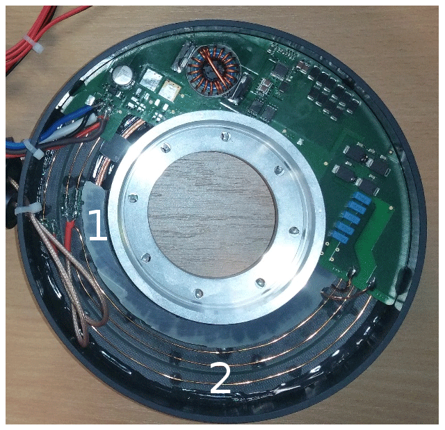
The parts marked as “2” are two data transfer coils, in this case simple wire loops, one for each direction of data transfer and again the same implementation being present at the energy receiving side, forming the data transfer channels for a full-duplex system. As these coils are formed by concentric loops with just a small gap, the rotation does just slightly affect the coupling factor between both sides. Anyway, the possibility for higher coupling factor variation due to the rotation and increased transfer distances will be addressed in Sect. 3.1 in addition to the static case.
As the data coils are just loosely coupled, dependent on the transfer distance, the signal loss is in the range of 10 to 15 dB. Additionally, noise is introduced to the data coils by the nearby energy transfer system, partly disturbing the data transfer. To improve the signal to noise ratio, the transfer losses between two corresponding data coils should be minimized. Nevertheless, for a comparably small transfer distance of 3 mm, 30 W of power can already be transferred simultaneously with a 100 Mbit s−1 Ethernet data stream using quadrature phase shift keying (QPSK) with a bandwidth of 62.5 MHz centred at 55 MHz (full-duplex, no frequency division multiplex), achieving a packet loss rate well below 1 %. The latter increases rapidly for higher transfer distances due to a reduced signal to noise ratio (mainly caused by the switched energy signal).
In the following chapters, we will examine the possibility to increase the data signal transfer distance by cancellation of the self-inductances of the data coils using non-Foster elements, namely negative inductors and thus reducing the path loss.
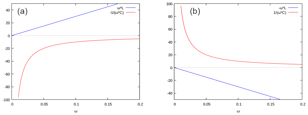
Foster's theorem (Foster, 1924) states that the reactance of any passive, lossless one-port circuit monotonically increases with frequency. It can be proven, including the case of low loss networks, based on the stored energy of a network or alternatively as a consequence of causality (Nedlin, 1989). In general, the derivative of a Foster reactance (or susceptance) over frequency is positive,
This behaviour is visualised in Fig. 2a) for a single inductance respectively a capacitance, showing the well-known plots for BL=ωL and . These basic circuit elements and all arbitrary combinations of both circuit elements can be considered as Foster reactances.
In contrast, networks not obeying Eq. (1) (non-Foster elements) yield a negative reactance (susceptance) slope over frequency. Analogous to the previous example, Fig. 2b) shows the reactance over frequency of a negative inductor () and a negative capacitor .
2.1 Non-Foster impedance transformation
An important result of Foster's reactance theorem can be found in impedance transformation networks. Let's consider an arbitrary, passive load impedance which should be matched to a purely resistive load. Besides the necessity of transforming the resistive part of the load impedance to the same value of the source resistance, the reactive part of the load must be compensated to achieve a matched state.
For simplicity, we further assume that the load's reactance is purely capacitive, so . To compensate this, a series inductor L could be inserted. As a consequence, depending on the inductance value, the load's reactance would be compensated for just exactly one frequency f0, where . With this implementation, the usable bandwidth is limited, a result well known from Fano's gain-bandwidth theory (Fano, 1948).
To overcome the limitations, non-Foster elements can be used, as they are able to compensate the load's reactance with the corresponding negated reactance. The usability of this approach has been shown in Sussman-Fort and Rudish (2009) for the matching of electrically short antennas, achieving an increased matched bandwidth and thus gain compared to conventional matching implementations.
2.2 Realisation of non-Foster elements
To achieve a non-Foster behaviour, at least one of the prerequisites of Foster's reactance theorem – losslessness and passivity – must be violated. In Au and Seo (2017), a passive non-Foster capacitance (−5 pF from 2.1 to 2.9 GHz) is reported, implemented as a Π-network of lumped resistors, inductors and capacitors. A negative inductance of approximately 2 nH in the same frequency range is described (Au and Seo, 2018), implemented as a dispersive transmission line. Without further proof, it can be stated that passive non-Foster implementations are intrinsically narrow band as they rely on frequency dependent, negative group delay networks, as used in the citations mentioned above.
A more common implementation of non-Foster elements is by using active elements like transistors or op amps forming a negative impedance converter (NIC), being able to negate a conventional. In for example Sussman-Fort and Rudish (2009), the first NIC circuit ever presented in Linvill (1953) has been used, employing two transistors in a feedback circuit.
Using op amps as an NIC significantly reduces the count of circuit elements, omits the complexity of transistor biasing and simplifies circuit analysis. Such circuits are presented in Marcellis et al. (2007) and have for example been used in Yang et al. (2009) to successfully match a resistively loaded V-dipole.
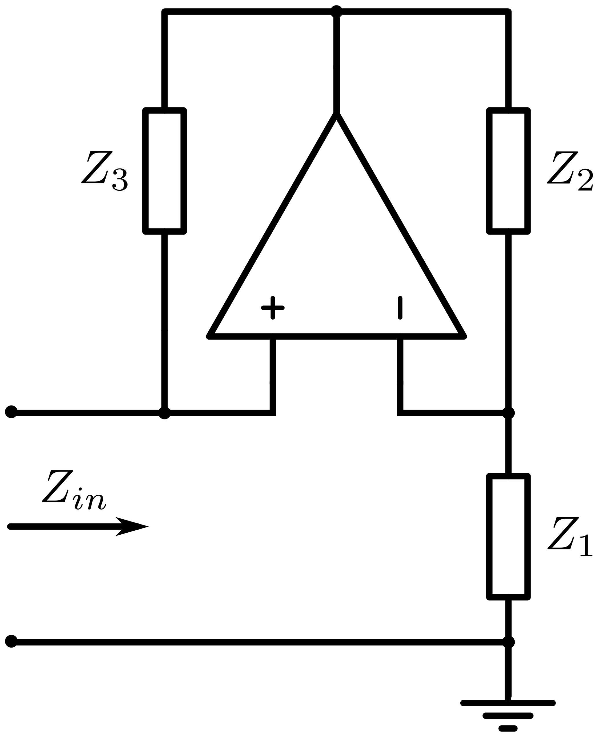
The basic circuit of an op amp based NIC is shown in Fig. 3, consisting just of the three impedances Z1, Z2, Z3 and the op amp itself. By simple circuit analysis, the input impedance Zin can be expressed as
Let's assume, Z2 and Z3 are purely resistive elements of the same value. The input impedance is consequently , or namely the non-Foster equivalent of the Foster impedance Z1. In general, we can convert any impedance Z1 into a scaled, negative version, dependent on the ratio .
As we will be using cascade matrices (or A-matrices) in the following chapters to mathematically model the impedance transformation of coupled inductors, the matrix representation given in Eq. (3) will be useful.
In this general representation, Kn is the converter constant (or scaling factor). In the case of our circuit, this constant equals . Consequently, the matrix represents only the highlighted part of Fig. 3 as two port network. Calculating the input impedance from an A-matrix is done using the following formula for general (complex) A-parameters (Steinbuch and Rupprecht, 1967). ZL represents the load impedance that terminates the two port network.
If we choose and ZL=R1, expectedly we end up with the same result as in Eq. (2).

As described in the introduction, the data transfer path in our systems is formed by loosely coupled inductors. A very basic, idealised equivalent circuit of such a transfer channel is shown in Fig. 4. Two inductors, L1 and L2 are coupled by their mutual inductance M with , k being the coupling factor. Due to the fact that the coupling factor k is much smaller than one, we cannot simply describe the impedance transformation of such an arrangement by the ratio of inductances or turns as it would be the case for an ideal transformer (with k=1). Subsequently, we need to investigate the impedance transfer by taking into account the non-unity coupling factor and the resulting input reactance.
3.1 Impedance transformation
To be able to describe the transfer behaviour mathematically, we use the equivalent T-circuit shown in Fig. 5.
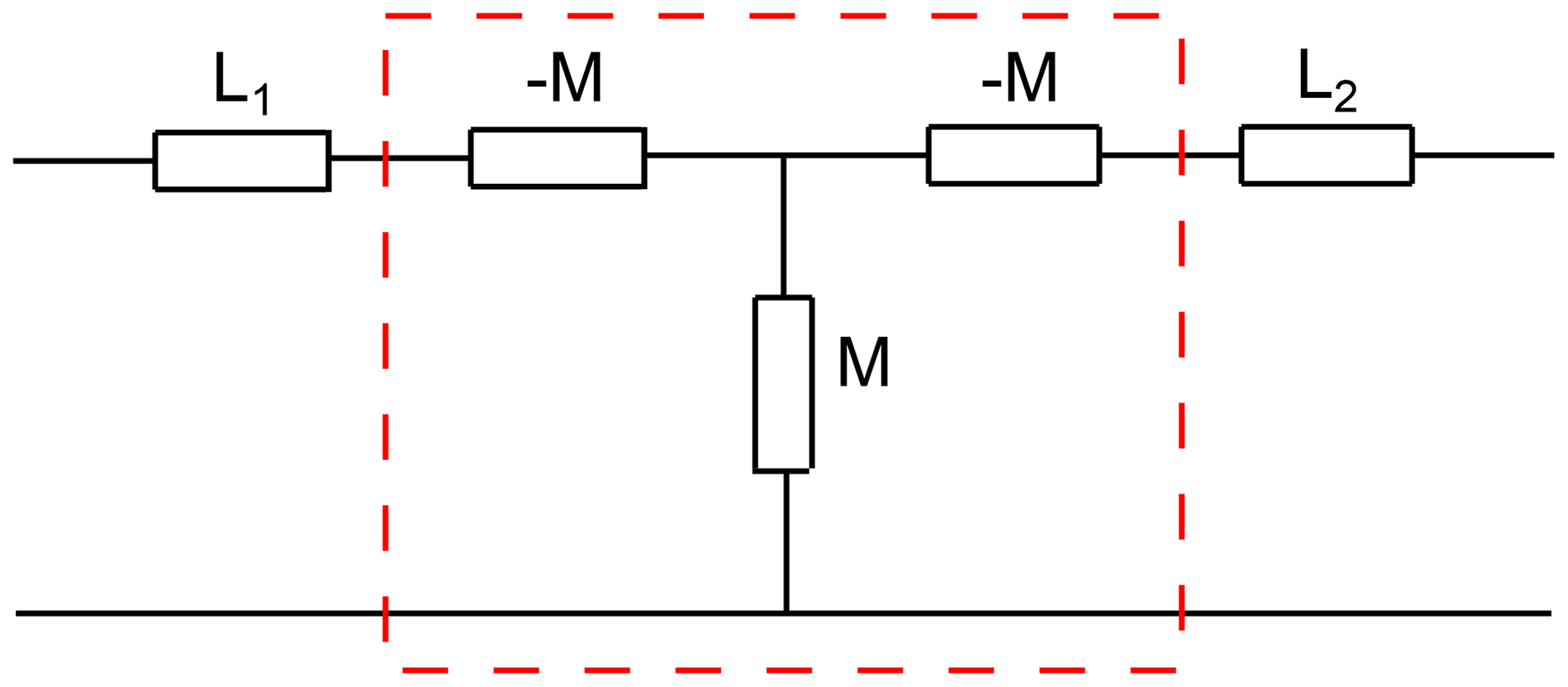
By using A-matrices, we can model this circuit as presented in the following equation:
Assuming a real load impedance RL connected to port two, using Eq. (4) we can further derive the resulting input impedance at port one as shown in Eq. (6).
From this result, we obtain a basic characteristic of loosely coupled inductors, namely the fact that they form an impedance inverter. The second coil's self inductance L2 is in series with the load resistance RL. At port one, the secondary impedance appears inverted and multiplied with the inversion factor K=ω2M2. This conversion can again be described by an A-matrix as shown in Eq. (7). Thus, the real load resistance's magnitude appears at port one as a frequency dependent value, which further complicates a broadband impedance matching.
To further examine the input impedance at port one, the real and imaginary part of Eq. (6) are given in the following expressions:
From Eq. (8), we see again the impedance inversion term. For high frequencies, we can omit the term in the denominator, so the real part approaches a constant value for increasing frequencies. A comparable assumption is true for the imaginary part, showing that the reactance of L1 dominates the total reactance. As L1 is in series with the transformed load resistance, they form a voltage divider. Subsequently, by compensating the reactance terms in Eq. (6), the signal transfer loss should be decreased.
An additional aspect to keep in mind is the increased complexity when dealing with non-constant transfer distances, thus variable coupling factor. Without further proof, it should be clear that the dependency between coil spacing and magnetic coupling is strongly non-linear. Additionally, the impedance transformations presented before are square-law dependent on the coupling factor, resulting in a broad range of possible input impedances for different transfer distances. As the inductive power and data transfer systems we focus on are, besides rotational motion, static, further investigations are out of the scope of this work. Nevertheless, the attempt to compensate the inductive part of the input impedance by use of Non-Foster elements is still applicable, especially as we have seen that the main reactive part of the input impedance is formed by the self inductance of the source side coil.
3.2 Reactance compensation methods
Assuming that we compensate the self inductances in Eq. (6), the modified input impedance would be purely real, as shown in the following equation.
Equation (10) shows that in the case of complete compensation of the self inductances, the modified input impedance is square-law dependent on the frequency, nevertheless, the input impedance is purely real.
One method of compensating the self inductances is the use of series or parallel capacitors, leading to loosely coupled resonating circuits as used for example in wireless energy transfer systems (Kurs et al., 2007). From the statements made in Sect. 2, it is clear that an inductor can only be compensated at exactly one frequency using a capacitive element, where . In case of coupled resonators, the mathematical description is quite extensive and would go beyond the scope of this paper. By calculating the zeros of the input impedance's imaginary part, three positive frequencies can be found for a symmetric system (equal inductors and capacitors). Besides the natural resonant frequency of the resonators, two coupling factor dependent solutions arise, which lead to the two well known transfer maxima in coupled resonator systems (frequency splitting phenomenon; Sample et al., 2011).
As a second method, non-Foster elements, namely negative inductors in series with the self inductances of the transfer system could be used. For ideal negative inductances, a frequency independent compensation of the coupled coils' reactance can be achieved. In this case, the input impedance would be exactly described by Eq. (10).
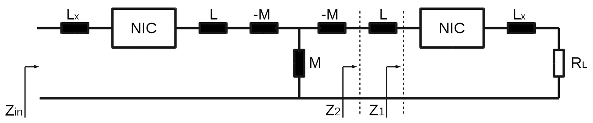
To verify the cancellation of the input reactance, we use a system as shown in Fig. 6. The loosely coupled inductors (planar loops of 50 mm diameter etched on FR4 material) in the centre are both of equal inductance (L=140 nH). Instead of using series non-Foster inductances, we use the circuit shown in Fig. 2 to negate a Foster (positive) inductance, thus cancelling the next series inductor. This approach is comparable to the one used in Yang et al. (2009).
Starting at the load resistance RL on the right, we have added a series inductance Lx, followed by the first negative impedance converter. At the reference plane (1), the impedance is . When choosing Lx=L, we achieve and impedance at reference plane (2), thus we will further refer to Lx as compensation inductance. Further following this scheme, we achieve an input impedance Zin equal to the expression in Eq. (10), with all reactive elements being cancelled out.
It is worth noting that all considerations so far were made under the assumption of ideal coupled inductors and especially ideal negative impedance converters. The following sections show that mainly the non-idealities of the op amps used as negative impedance converters lead to significant deviations from the ideal case.
4.1 Simulation
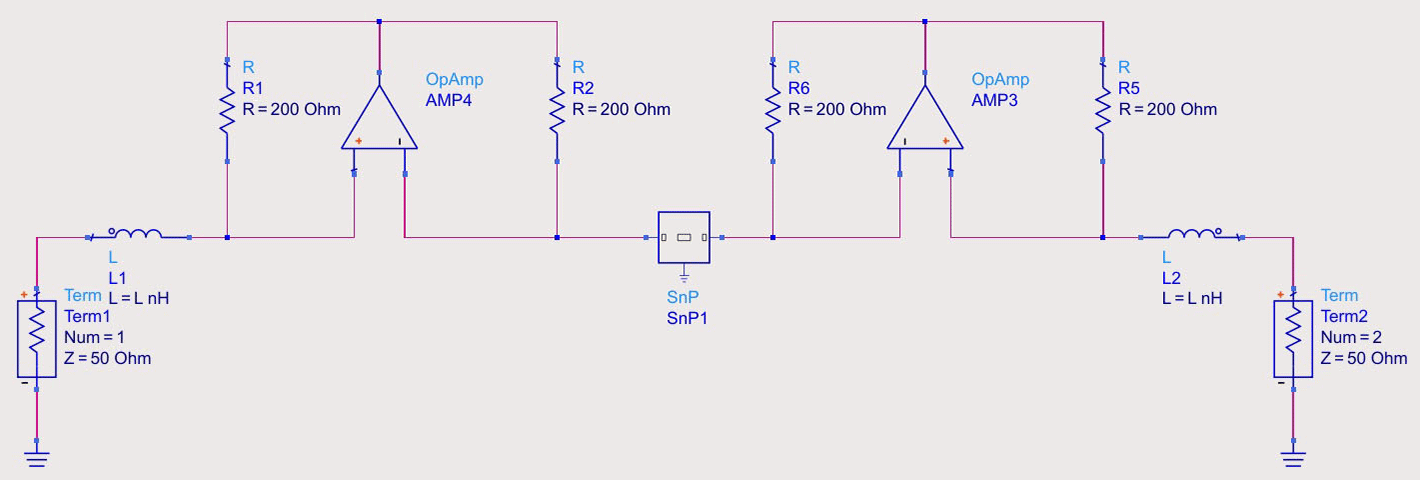
To verify the reactance cancellation approach described before, a schematic S-parameter simulation has been carried out in Keysight Advanced Design System. The simulated schematic in Fig. 7 is built analogous to the block diagram presented in the section before. The central part (SnP1) is a touchstone file block containing the two port representation of the measured coupling coils. As such, the parasitic effects of the real coupled inductors is taken into account while the negative impedance converters are built using ideal components.
The inductances L1 and L2 in the schematic have initially been set to the measured self-inductance of the coupling coils and subsequently been simultaneously tuned to 142.6 nH to achieve the S11 plot shown in Fig. 8.

For comparison, the S11 measurement of just the coupled data transfer coils is also shown (blue trace). The reactive part of the system, caused by the self-inductances of the coupling coils, has been almost completely compensated by adding negated inductors of the same magnitude. The resulting reflection coefficient and thus the input impedance of the system is almost purely real, yet the magnitude shows a frequency dependency.
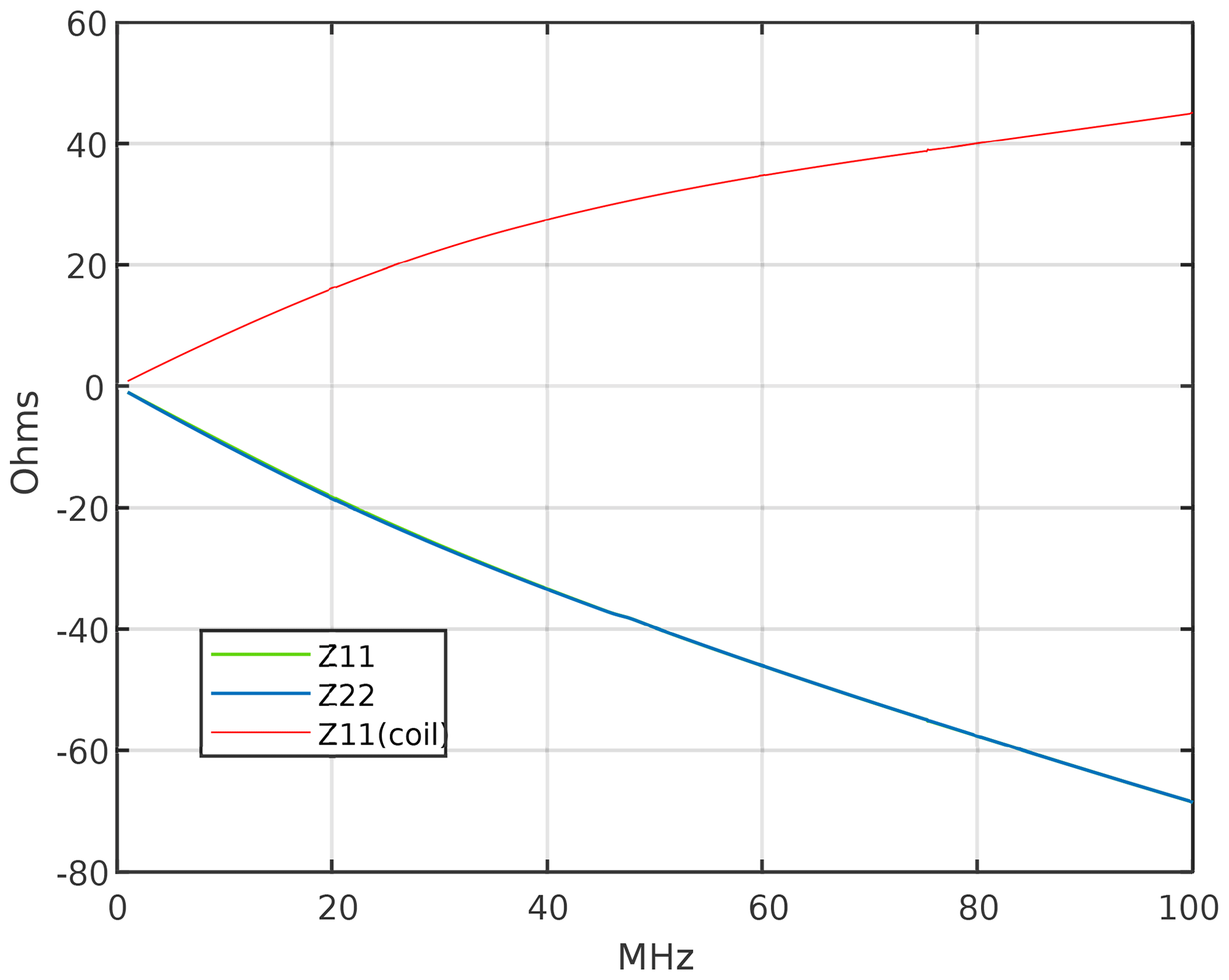
Looking at the Z-parameter plots in Fig. 9, this frequency dependency of the real part shows the square law transformation due to the impedance inverter formed by the coupled coils as described by Eq. (10).
As we have simulated the system using measured data of the coupled coils and an ideal implementation of the negative impedance converters, the results presented so far have shown the maximally achievable system performance regarding reactance cancellation.
4.2 Measurement results
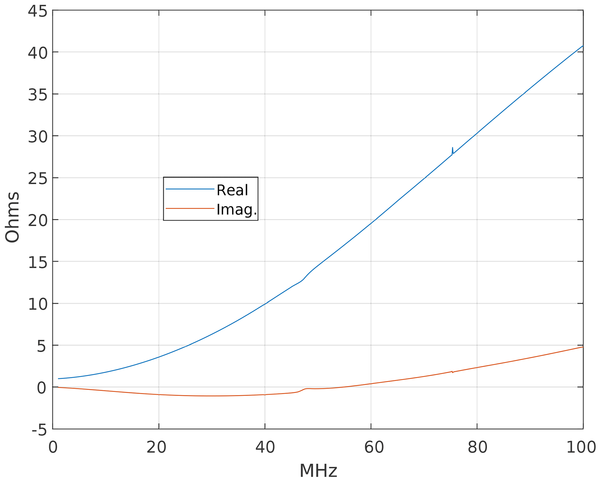
The system described before has been built using the op amp OPA684 by Texas Instruments in the NIC circuit, promising a high open-loop gain and bandwidth as needed for the NIC to work correctly. As a first step, the input impedances of the NIC circuits connected to the coupling coils have been measured. For comparison, Fig. 10 also shows the imaginary part measured at the coupling coils alone (red trace).
The plot shows the expected non-Foster behaviour, namely the negative (almost) linear slope of a negative inductor. As next step, the compensation inductances have been added to the NIC circuit. The measured input reactance of both ports is shown in Fig. 11, again with the reactance of the coupling coil alone for comparison (blue trace). The reactance of the system is in good agreement with the simulated results in Fig. 9.

Consequently, the setup shows the expected behaviour regarding the cancellation of the coupling coils' self-inductance.
In contrast, regarding the transformation of the load resistance, the setup shows a non-ideal behaviour as can be seen from Fig. 12. Though the measured reflection coefficients are almost purely real and a frequency dependent behaviour can be seen in the plot, the real part has an offset of four units, which is equal to 200 Ω.

As this is just the value of the feedback resistors of our circuit, it can be concluded, that the parameters of the op amp like open loop gain and bandwidth are possibly too low. Followingly, the circuit adds a real component as described in Yang et al. (2009) as a result of a non-ideal op amp.
It was tried to achieve the same behaviour in simulation by degrading the gain and bandwidth of the op amps, but without being able to fully depict the measurement results. A simulation model of the op amp used exists but just as spice model which cannot be used in an s-parameter simulation. Additionally, the frequency behaviour and roll-off of the gain cannot be portrayed in the simulation, just a constant, frequency independent value. Further investigations are needed to find the cause, possibly parasitic effects not directly covered by the simulation parameters.
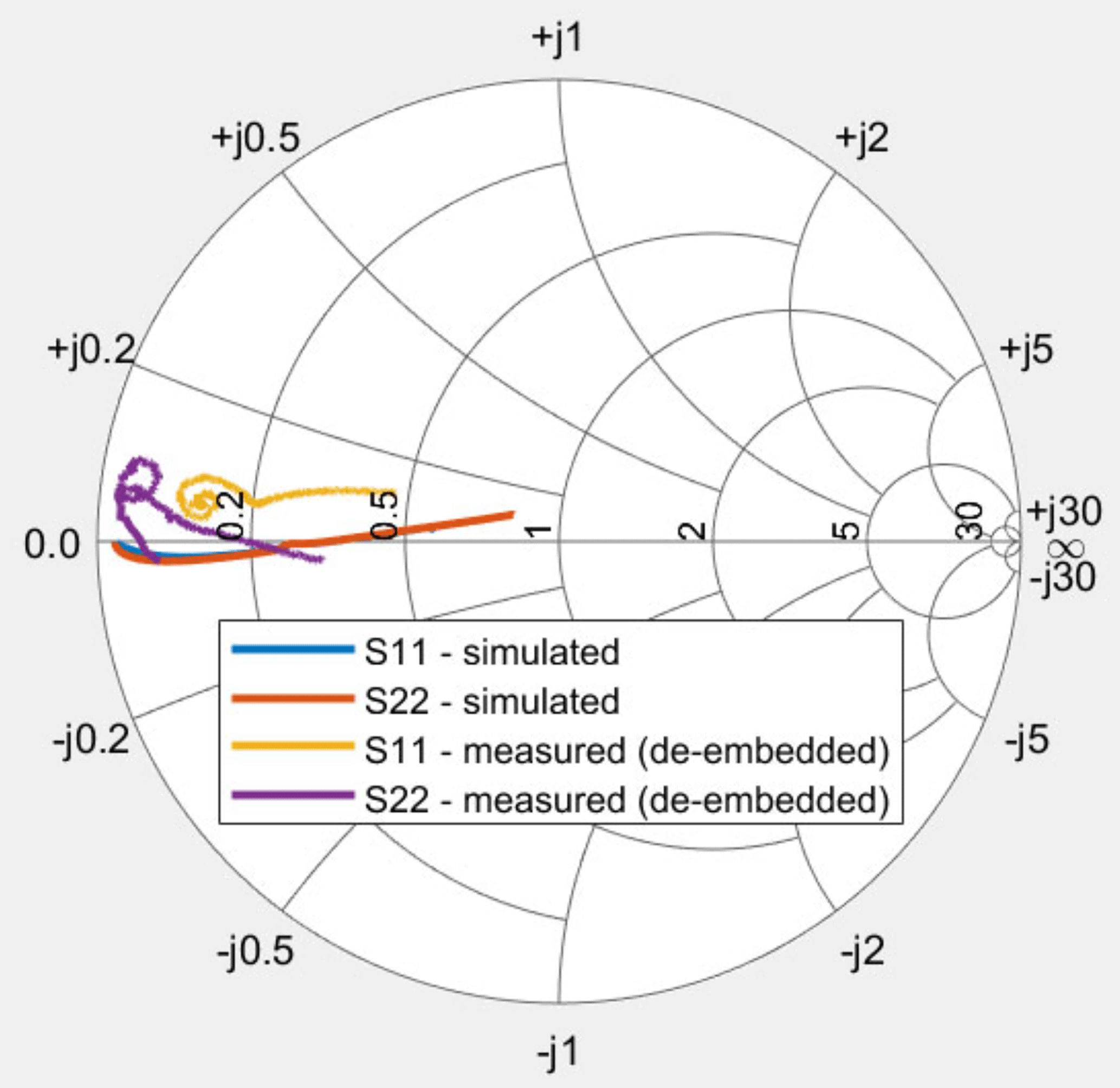
To be able to compare the system's behaviour regarding the reactance cancellation, a post processing step has been made, substracting the 200 Ω offset from the measured S-parameters (de-embedding). As can be seen from Fig. 13, the resulting plots are in comparably good agreement with the simulation.
In conclusion, besides the offset in the real part, the principle of reactance cancellation works for loosely coupled inductors. More effort must be spend to improve the NIC circuits behaviour to finally be able to achieve an improved signal transfer and impedance matching over a certain bandwidth.
In this paper, a concept to compensate the reactive part of loosely coupled inductors used to transfer data has been presented. Negative impedance converter circuits have been used to successfully negate the coils' self-inductance and compensate it using additional series inductances. Further effort must be spend on the optimisation of the circuit to eliminate the additional resistive part introduced by the NICs in the measurements. By achieving this, inductive data links can be optimised regarding signal transfer loss and impedance matching. The transfer distance of the system presented in the introduction could be increased with sufficiently small bit error rate. As a new idea, in a certain frequency range, the matching achieved could be high enough to achieve bi-directional transfer using just one pair of coils by inserting (active) circulators to separate the two transfer directions.
Measurement data is available in the Supplement.
The supplement related to this article is available online at: https://doi.org/10.5194/ars-17-151-2019-supplement.
The main idea for this work was contributed by CS. He also did simulation, implementation and measurement tasks. MB and MC supported with fruitfull discussions and result interpretations. MB supported also with data post-processing and plotting.
The authors declare that they have no conflict of interest.
This article is part of the special issue “Kleinheubacher Berichte 2018”. It is a result of the Kleinheubacher Tagung 2018, Miltenberg, Germany, 24–26 September 2018.
We thank IST – Ingenieurbüro für Sensortechnik GmbH for their support in this project.
This research has been supported by the Bundesministerium für Wirtschaft und Technologie (grant no. ZF4050305PRG).
This paper was edited by Jens Anders and reviewed by two anonymous referees.
Au, N. and Seo, C.: Novel design of a 2.1–2.9 GHz negative capacitance using a passive non-Foster circuit, IEICE Electronics Express, 14, 1–6, https://doi.org/10.1587/elex.13.20160955, 2017. a
Au, N. and Seo, C.: A design of passive negative shunt inductance circuit using negative group delay network, IEICE Electronics Express, 15, 1–9, https://doi.org/10.1587/elex.15.20180428, 2018. a
Chen Gong, Dake Liu, Z. M. W. W., and Li, M.: An NFC Two-Coil WPT Link for Implantable Biomedical Sensors under Ultra-Weak Coupling, Sensors, 17, 1–20, https://doi.org/10.3390/s17061358, 2017. a
Daerhan Liu, Kun Bao, Y. S., and Georgakopoulos, S. V.: Simultaneous Wireless Power and Data Transfer Through Broadband CSCMR, 2018 IEEE International Symposium on Antennas and Propagation & USNC/URSI National Radio Science Meeting, pp. 2535–2536, https://doi.org/10.1109/APUSNCURSINRSM.2018.8608244, 2018. a
Fano, R. M.: Theoretical Limitations on the Broadband Matching of Arbitrary Impedances, Technical Report, Elsevier Ltd, Journal of the Franklin Institute, No. 41, 1948. a
Foster, R. M.: A reactance theorem, The Bell System Technical Journal, 3, 259–267, https://doi.org/10.1002/j.1538-7305.1924.tb01358.x, 1924. a
Guillaume Simard, M. S. and Massicotte, D.: High-Speed OQPSK and Efficient Power Transfer Through Inductive Link for Biomedical Implants, IEEE T. Biomed. Circ. S., 4, 192–200, 2010. a
Guoxing Wang, Peijun Wang, Y. T., and Liu, W.: Analysis of Dual Band Power and Data Telemetry for Biomedical Implants, IEEE T. Biomed. Circ. S., 6, 208–215, https://doi.org/10.1109/TBCAS.2011.2171958, 2011. a
Guoxing Wang, Xiyan Li, M. W. H. Y., and Xu, W.: Optimization of a Dual Band Wireless Power and Data Telemetry System Using Genetic Algorithm, IEEE Design & Test, 35, 54–65, https://doi.org/10.1109/MDAT.2016.2582828, 2016. a
Hao Hu, S. V. G.: Multiband and Broadband Wireless Power Transfer Systems Using the Conformal Strongly Coupled Magnetic Resonance Method, IEEE T. Ind. Electron., 64, 3595–3607, https://doi.org/10.1109/TIE.2016.2569459, 2017. a
Hoeher, P. A.: FSK-based Simultaneous Wireless Information and Power Transfer in Inductively Coupled Resonant Circuits Exploiting Frequency Splitting, IEEE Access, 7, 40183–40194, https://doi.org/10.1109/ACCESS.2019.2907169, 2019. a
Hongchang Zheng, Zhihui Wang, Y. L., and Deng, P.: Data Transmission through Energy Coil of Wireless Power Transfer System, 2017 IEEE PELS Workshop on Emerging Technologies: Wireless Power Transfer (WoW), https://doi.org/10.1109/WoW.2017.7959373, 2017. a
Jiande Wu, Chongwen Zhao, Zhengyu Lin, Jin Du, Yihua Hu, and Xiangning He: Wireless Power and Data Transfer via a Common Inductive Link Using Frequency Division Multiplexing, IEEE T. Ind. Electron., 62, 7810–7820, https://doi.org/10.1109/TIE.2015.2453934, 2015. a
Kurs, A., Karalis, A., Moffatt, R., Joannopoulos, J. D., Fisher, P., and Soljacic, M.: Wireless Power Transfer via Strongly Coupled Magnetic Resonances, Science, 317, 83–86, 2007. a
Linvill, J.: Transistor Negative-Impedance Converters, Proc. I.R.E., 41, 1953. a
Mandal, S. and Sarpeshkar, R.: Power-Efficient Impedance-Modulation Wireless Data Links for Biomedical Implants, IEEE T. Biomed. Circ. S., 2, 301, https://doi.org/10.1109/TBCAS.2008.2005295, 2008. a, b
Marcellis, A. D., Ferri, G., and Stornelli, V.: NIC-based capacitance multipliers for low-frequency integrated active filter applications, 2007 PhD Research in Microelectronics and Electronics Conference, IEEE, Bordeaux, 2007. a
Nedlin, G.: Energy in lossless and low-loss networks, and Foster's reactance theorem, IEEE T. Biomed. Circ. S., 36, 259–267, https://doi.org/10.1109/31.92888, 1989. a
Peijun Wang, Yina Tang, H. W., and Wang, G.: A Novel Overlapping Coil Structure for Dual Band Telemetry System, 2012 IEEE International Symposium on Circuits and Systems, https://doi.org/10.1109/ISCAS.2012.6271724, 2012. a
Sample, A. P., Meyer, D. A., and Smith, J.: Analysis, Experimental Results, and Range Adaptation of Magnetically Coupled Resonators for Wireless Power Transfer, IEEE T. Ind. Electron., 58, 544–554, 2011. a, b
Steinbuch, K. and Rupprecht, W.: Nachrichtentechnik, Springer Verlag, Berlin/Heidelberg/New York, 1967. a
Sussman-Fort, S. E. and Rudish, R. M.: Non-Foster impedance matching of electrically-small antennas, IEEE T. Antenn. Propag., 57, 2230–2241, https://doi.org/10.1109/TAP.2009.2024494, 2009. a, b
Wang, G., Liu, W., Sivaprakasam, M., Zhou, M., Weiland, J. D., and Humayun, M. S.: A Dual Band Wireless Power and Data Telemetry for Retinal Prosthesis, Proceedings of the 28th IEEE EMBS Annual International Conference, New York City, USA, 30 August–3 September 2006, pp. 4392–4395, https://doi.org/10.1109/IEMBS.2006.260470, 2006. a
Xiaofei Li, H. W. and Dai, X.: A Power and Data Decoupled Transmission Method for Wireless Power Transfer Systems via a Shared Inductive Link, Energies, 11, 2161, https://doi.org/10.3390/en11082161, 2018. a
Yang, H. E., Kim, I., and Kim, K.: Non-Foster impedance matching of electrically-small antennas, IEEE T. Antenn. Propag., 57, 2230–2241, https://doi.org/10.1109/TAP.2009.2024494, 2009. a, b, c
Zhou, M., Liu, W., Wang, G., Sivaprakasam, M., Yuce, M. R., Weiland, J. D., and Humayun, M. S.: A Transcutaneous Data Telemetry System Tolerant to Power Telemetry Interference, 2006 International Conference of the IEEE Engineering in Medicine and Biology Society, pp. 5884–5887, https://doi.org/10.1109/IEMBS.2006.260803, 2006. a