 | 19 Sep 2019
10-bit tracking ADC with a multi-bit quantizer, variable step size and segmented current-steering DAC
Stefan Bramburger
Dirk Killat
This paper presents a 10-bit tracking ADC using a multi-bit quantiser and a segmented current-steering DAC. The quantiser allows a dynamical adjustment of the step size dependent on the input signal waveform. This mitigates the limited slew rate of delta encoded ADCs. Energy consumption induced by 1 LSB ripple is removed by the quantiser. The segmented current-steering DAC allows simple control, good monotonicity and improved transient response when compared to previous design as well as potential power reduction.
- Article
(7525 KB) - Full-text XML
-
Supplement
(51 KB) - BibTeX
- EndNote


Several different topologies exist for ADCs. The type of tracking ADCs is located between nyquist rate and delta sigma ADCs according to their sample rates. The main advantage is, that one conversion per clock cycle is achieved. The main drawbacks of tracking ADCs are the limited slew rate and the output ripple. The slew rate can be enhanced by increasing the clock rate (Huang, 2013a), which would also increase the energy consumption. A better option is to increase the step size of the ADC. The presented ADC (Fig. 1) has a sample rate of up to 50 MS s−1 and a variable step size of 1 or 2 LSB steps which is achieved by a multi-bit quantiser (Shaker, 2010). The ripple of the output signal is caused by toggling the DAC by 1 LSB every clock cycle when the input amplitude varies less than 1 LSB. This problem is also solved with the quantiser used here.

A current-steering DAC can be used in the feedback path. To achieve higher resolutions with good performance it is necessary to segment the feedback DAC (Moody, 2014). In the ADC presented here the DAC is segmented into 3-bit binary encoded registers and 7-bit thermometer encoded registers. A binary encoding has the advantage of short conversion time, though also has worse monotonicity at higher resolutions. The MSBs are therefore thermometer encoded, which has a better monotonicity and means that less effort is required for error compensation (McDonnell, 2017). A drawback of this type of encoding is a slower transition, though this is less essential for MSBs. The main disadvantage, however, is that a binary to thermometer decoder is needed, which would increase the power consumption (Radulov, 2006; Nazari, 2016). In order to avoid having to use this decoder a control with an up/down signal is implemented. This is well suited for tracking ADCs, due to their limited slew rate. An application example for a tracking ADC is shown in Kanzian (2018). It is used in a controller of a dc-dc converter.
This paper is organised as follows: Sect. 2 describes the ADC's components, Sect. 3 describes the layout of the DAC and comparators, Sect. 4 presents simulation results and finally Sect. 5 provides a brief conclusion.
The ADC presented in Fig. 1 comprises, apart from the multi-bit quantiser and the 10-bit current-steering DAC which are discussed in the following, a digital counter. The digital counter generates the control signals for the DAC and provides the binary output, the supply voltage for all circuits is 1.2 V.
2.1 Multi-bit quantiser
The multi-bit quantiser consists of 4 comparators. One comparator circuit is given in Fig. 2. The quantiser level is realised by programming comparator offset. Both input ports are connected to source followers and resistor chains. Resistors of 1 kΩ are used to generate identical voltage offsets in steps of 1 LSB. The eight switches connect the latch stage common source input to the source follower buffer's selected resistor tap. The switching levels are ±1 VLSB and ±3 VLSB. Table 1 gives a summary of realised comparator levels and the required switch connectivity. Another feature of the comparators is the reduced kickback noise during the settling phase of the latch stage (Huang, 2013b). The transistors with the XOR-signal at the gate therefore disconnect the inputs from the analog outputs. The logic following the latch generates the XOR-signal and a stable output during the reset phase of the comparator.
Table 1 provides an overview of the different comparators' switching levels as well as the resulting step sizes. In order to count up one step, comparator number 1 (+3 VLSB) must be at zero while all others have to be at 1. For zero step size, which is important for ripple cancellation, the first two comparators have to be at zero, with the other two at 1. The remaining levels count up by 2 steps, then down by 1 and again down by 2 are described in Table 1.
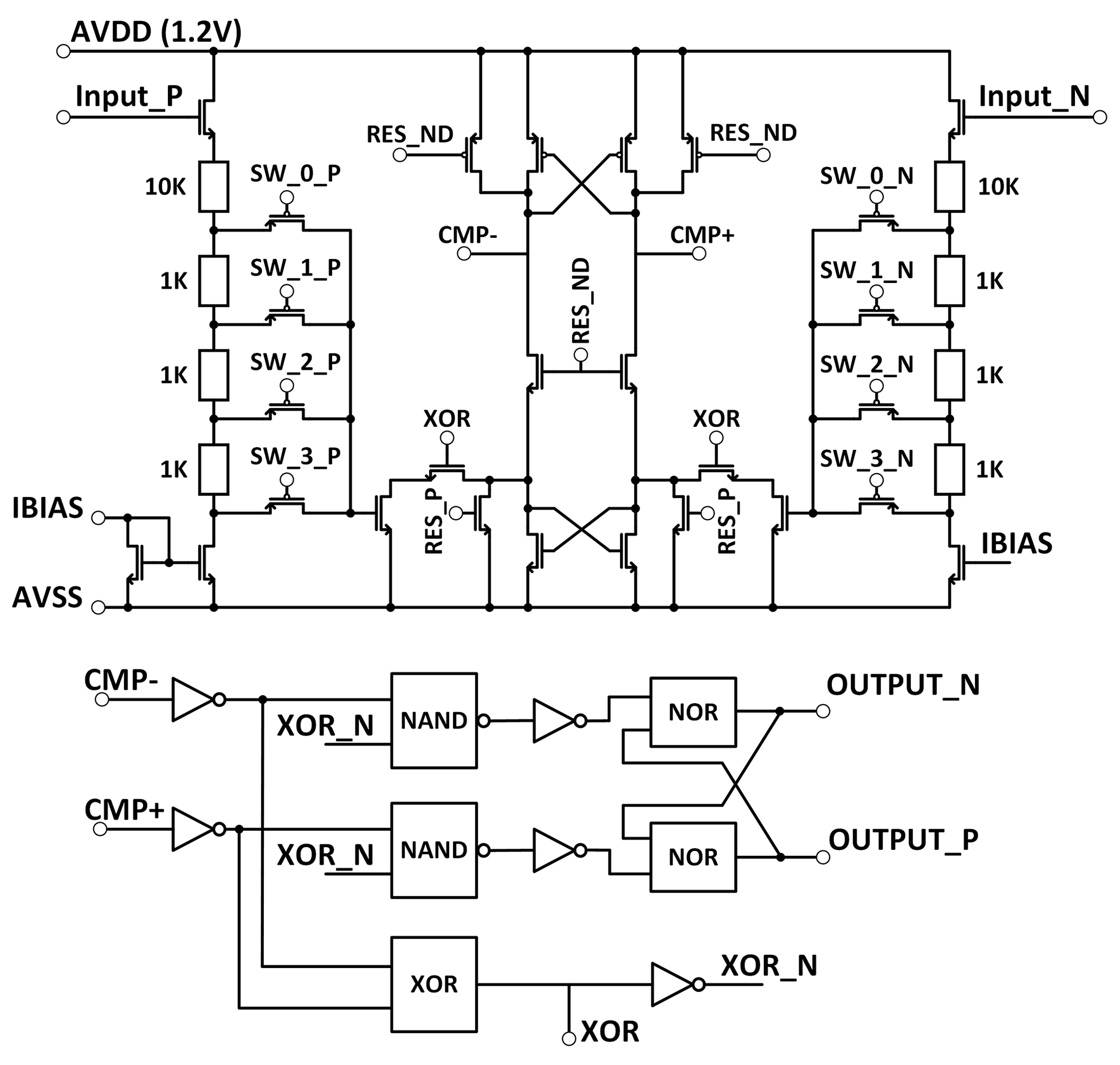
Table 1Overview of the quantiser level, the closed switches in a comparator attaining the desired level, the comparators's output and the resulting step size and direction of the DAC.

2.2 Current-steering DAC
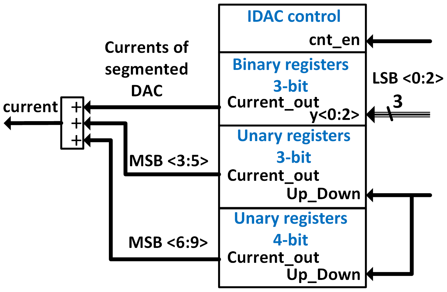
An overview of the current-steering DAC is shown in Fig. 3. The DAC consists of four parts: the IDAC control, a 3-bit binary coded register, a 3-bit unary coded register and a 4-bit unary coded register. The digital counter (Fig. 1) delivers the control signals cnt_en and Up_Down. The three LSBs y〈0:2〉 of the counter's output are directly connected to the 3-bit binary coded register. The IDAC's output current is fed back into the ADC's input, which is also differential.
The 3-bit binary coded register consists of 7 current sources, where each has an output current of I = 100 nA. This register is directly controlled by the digital counter's 3 LSB. The 3-bit unary coded register consists of 7 current sources with a unit current of I = 800 nA while the 4-bit unary coded register has 15 current sources where I = 6.4 µA per source. The Up_Down signal, which is connected to the unary registers, controls the direction of switching. The cnt_en signal activates the switching of the unary registers in IDAC control. IDAC control then operates the current sources in unary coded register sections.
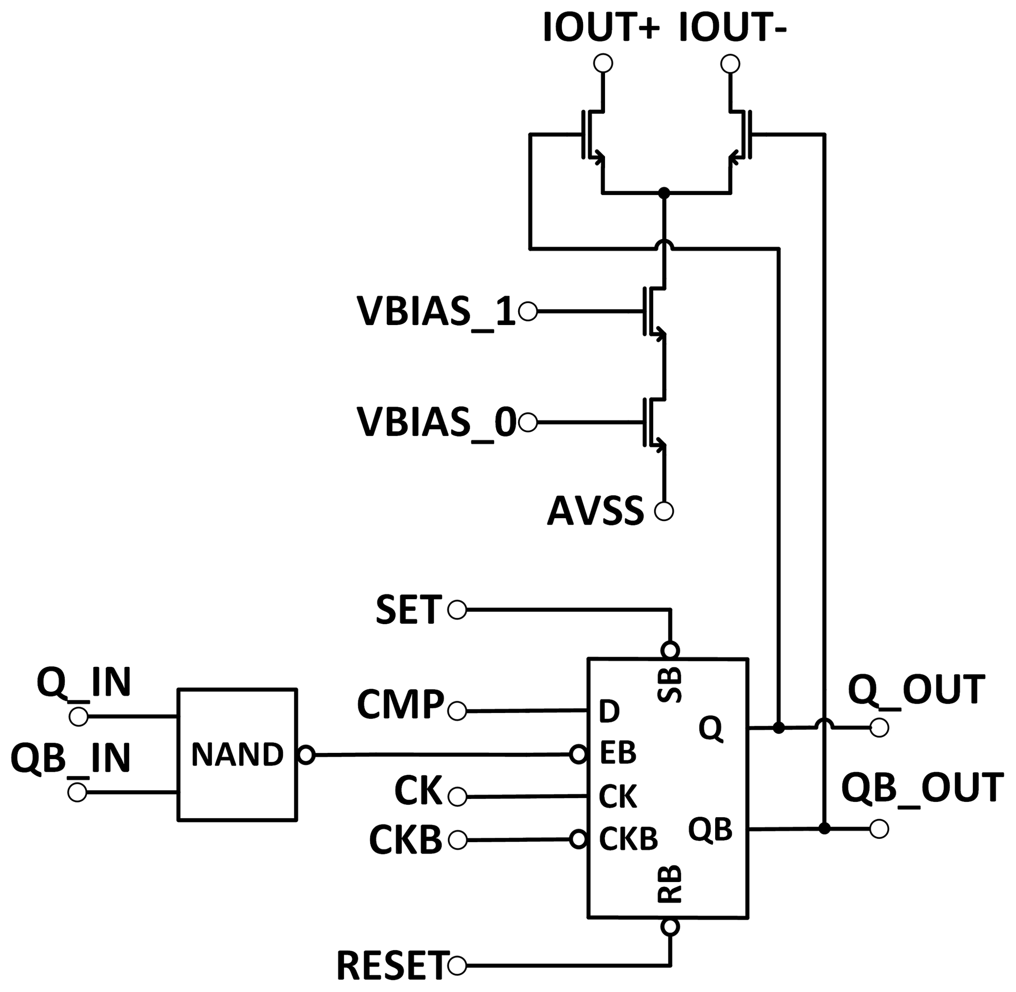
The DAC unit cell's schematic is presented in Fig. 4. The analog part consists of a current source and a switch. The current source is cascaded and biased for low voltage output. The differential switch connects the source either to the positive or negative output current rail. The switches are controlled by a flip-flop, enabled by Q_IN and QB_IN through a NAND gate. In the unary coded register section these inputs are connected between the previous unit cell output and the next unit cell input. This allows for a sequential switching of the DAC cells. In the binary coded register section the flip flop is always enabled. The flip-flop can be set with the CMP input signal from the comparator.
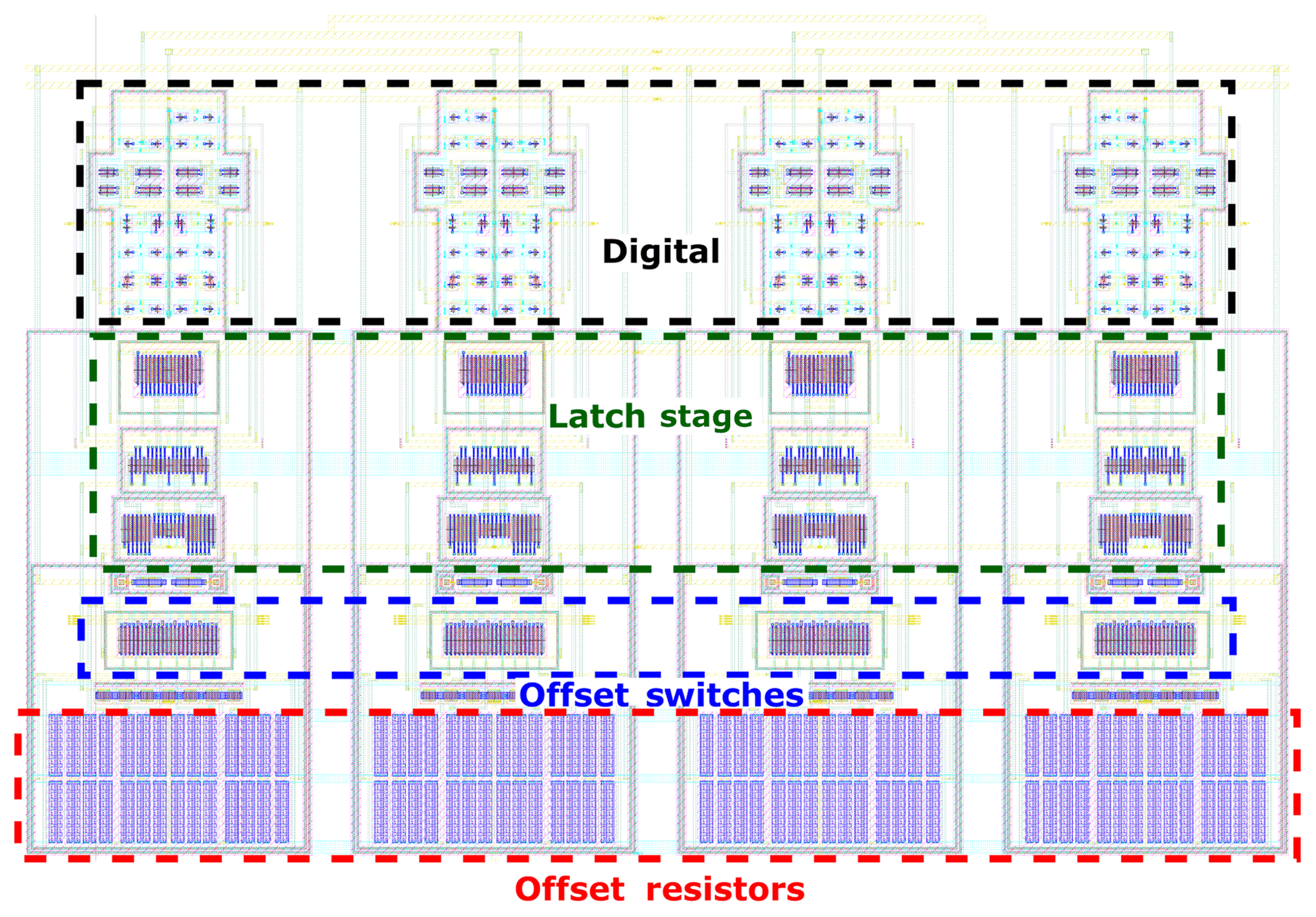
The circuit is designed using a 65 nm low-power CMOS technology of TSMC. The four comparators are shown in Fig. 5. All comparators have a dimension of 98 µm × 60 µm. From the bottom to the top the layout depicts the offset resistors at the input, the offset switches that connect the input with the latch stage, the analog part, and finally a digital output and serial connection of registers. In Fig. 6 the layout of the current-steering DAC is depicted. It has a dimension of 130 µm × 169 µm. The registers' current sources are arranged symmetrically so as to achieve a good monotony. All sections of registers have their own biasing network.

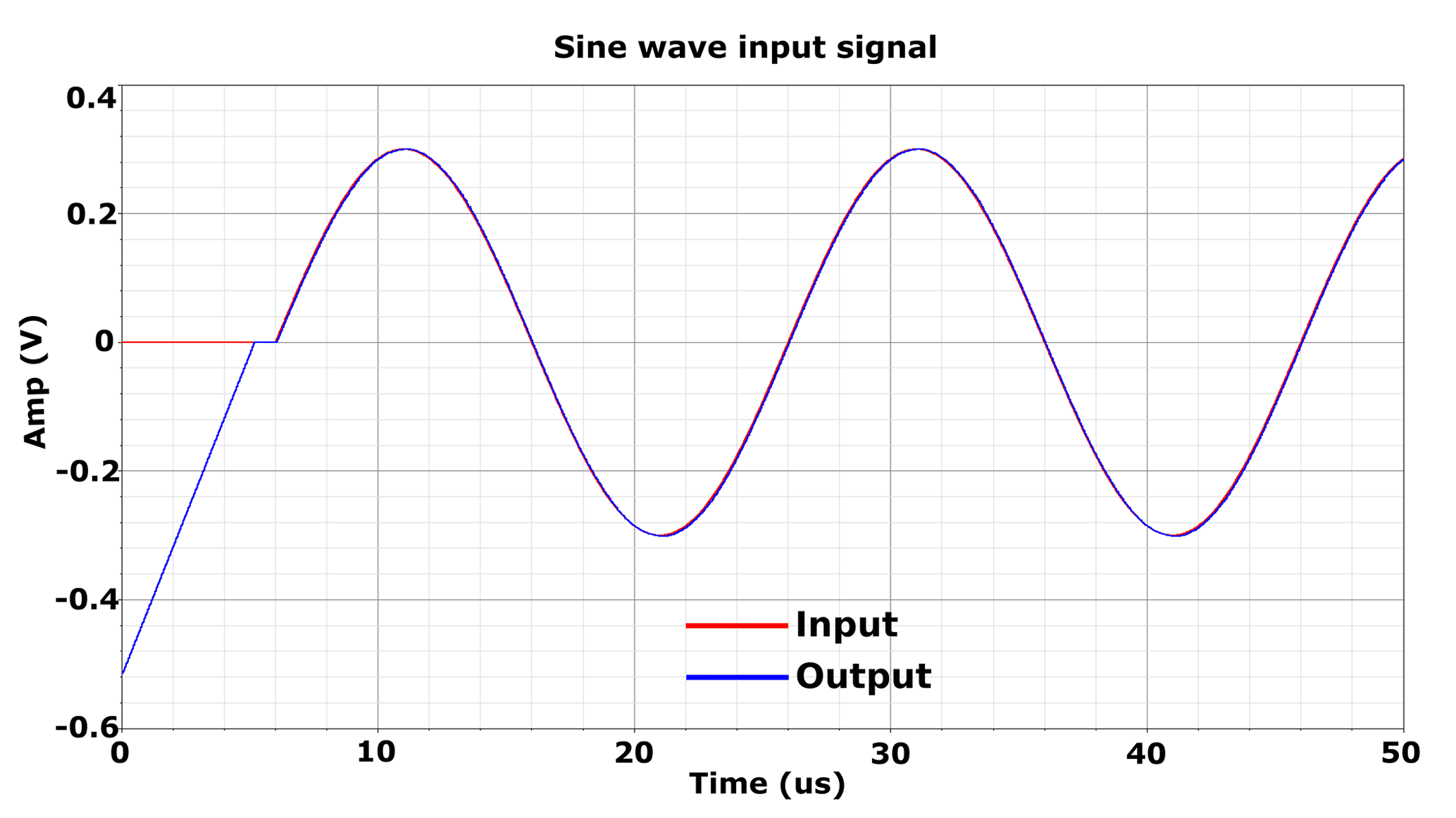
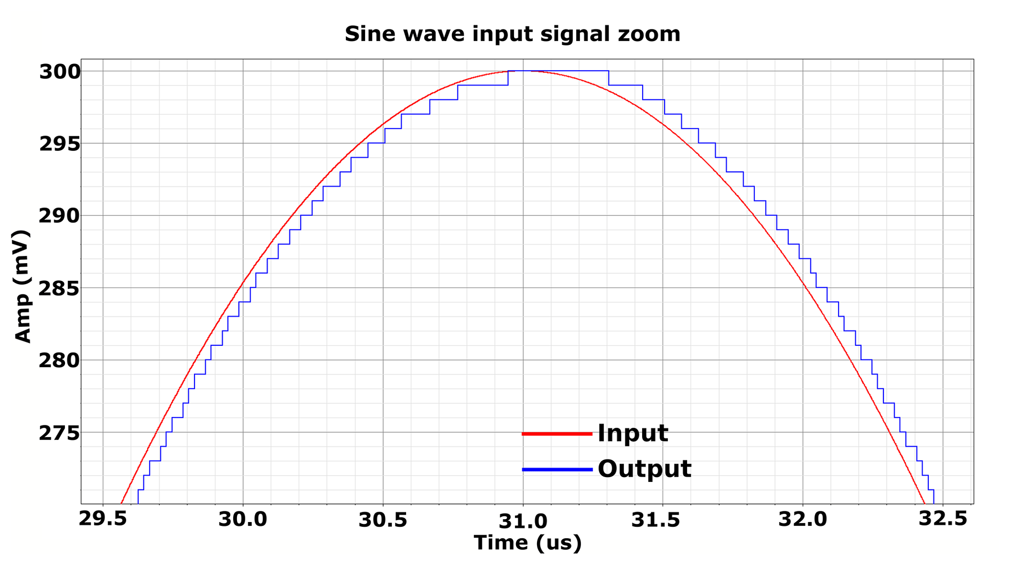
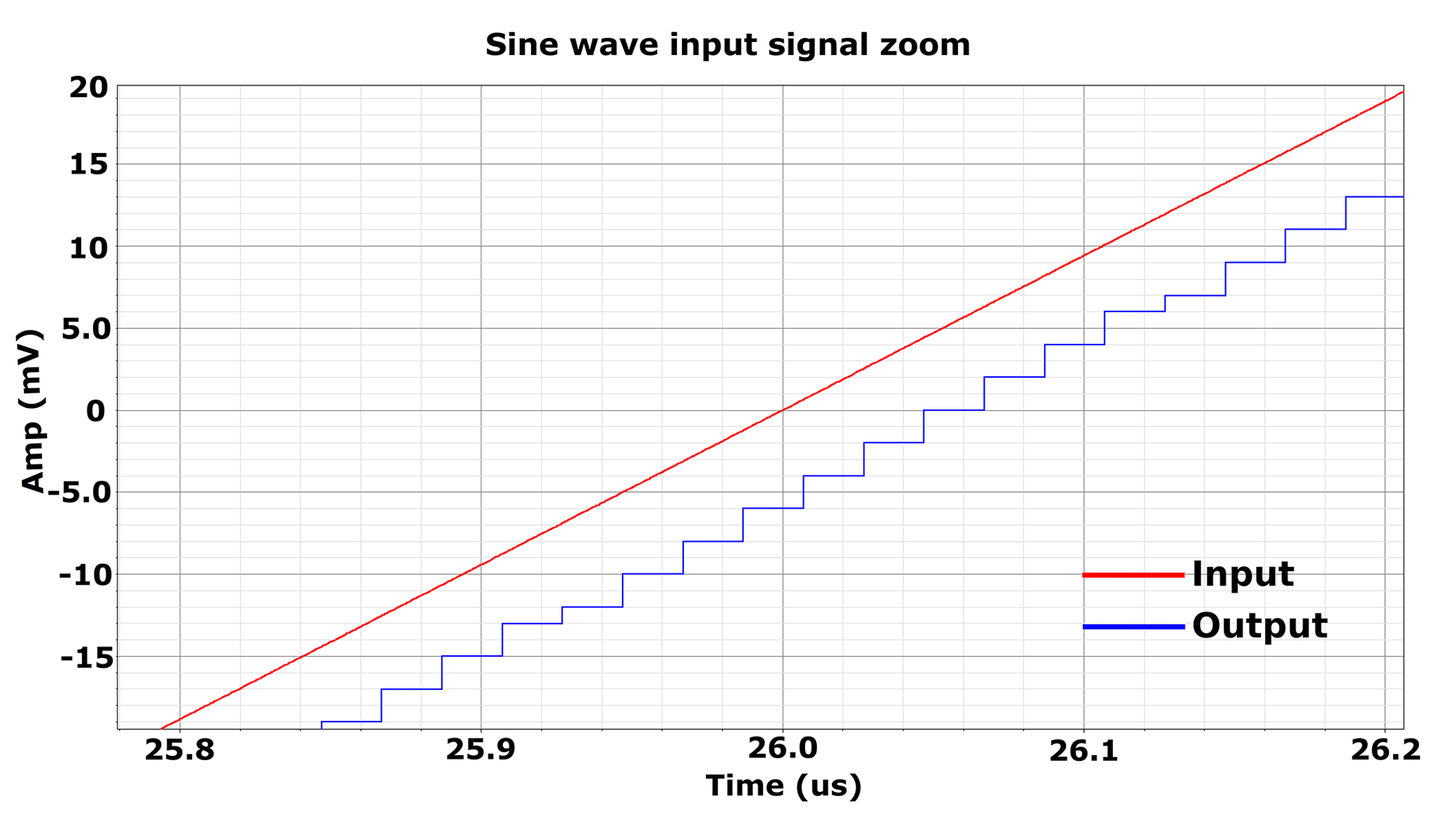
Large signal transient transistor level simulation results are discussed in Figs. 7 to 11. The input signal in Fig. 7 is a sine wave with a frequency of fSIG = 50 kHz and an amplitude of VAMP = 300 mV. The LSB voltage is VLSB = 1 mV and the system frequency is fCLK = 50 MHz, which is the fCLK = 50 MHz, which is the maximum sample rate. 5 µs the ADC has to compensate the DC input signal as after reset the DAC is set to its minimum value. After start-up the ADC is able to convert the input signal. Figure 8 depicts a closeup of the sine wave peak. Step sizes of 1 and 0 LSBs can be observed. This results in a constant output signal over several clock cycles. Figure 9 illustrates the input signal's the steepest gradient. Step size is here increased to 2 LSB.
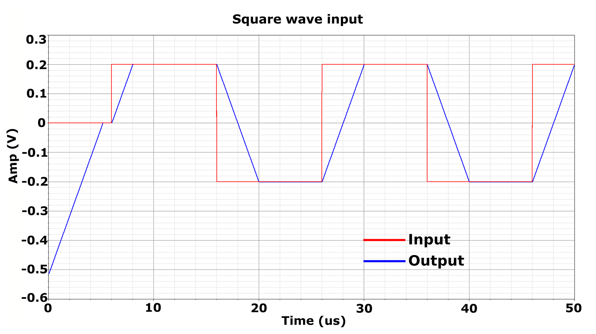
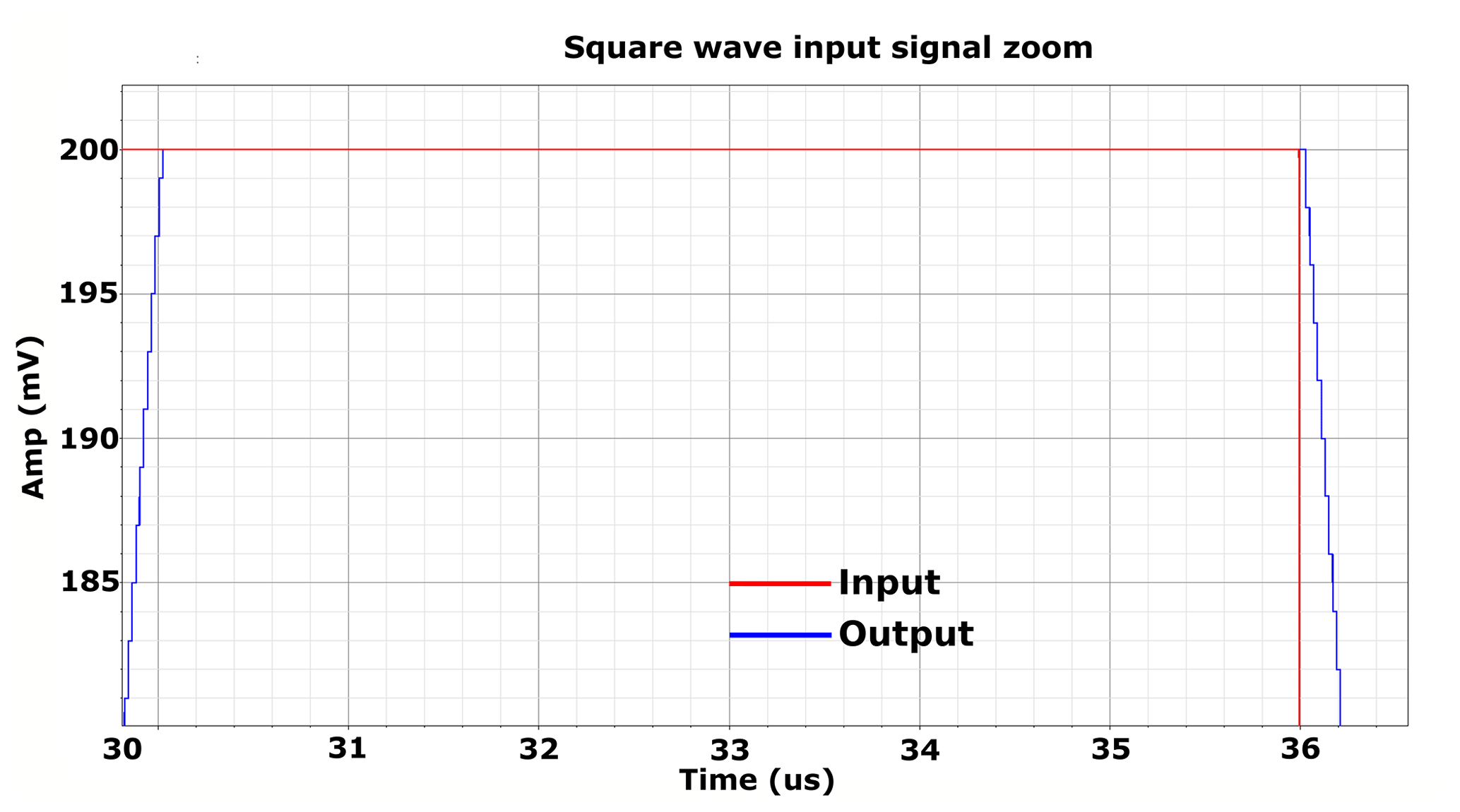
The second input signal (Fig. 10) is a square wave with a frequency of fSIG = 50 kHz and an amplitude of VAMP = 200 mV. The LSB's voltage and the system frequency is the same as in the previous simulation. After start-up and the first rising edge of the input, the ADC enters the fastest mode with a slew rate of 2 mV/20 ns. The major problem of tracking ADCs is the limited slew rate, and in this case it has already improved by a factor of 2. A closeup of the square wave is depicted in Fig. 11. The second major disadvantage of tracking ADCs is the ripple of the output signal. Even with a constant input signal there is a ripple of 1 LSB. The proposed ADC does not have this ripple due to the zero step size when deviation from ideal conversion is less than 1 LSB (step size 0 in Table 1. The simulation result presented in Fig. 11 shows the ripple-free ADC output signal.
Simulations for different input frequencies are captured in Table 2. In addition, the signal amplitude is varied. Due to the higher slope of the input signal, lower frequencies are converted for higher amplitudes. The SNDR was measured and calculated in the time domain with Eq. (1).
Table 2Results for varied input frequencies and signal amplitudes (VLSB = 1 mV) (system level simulation).
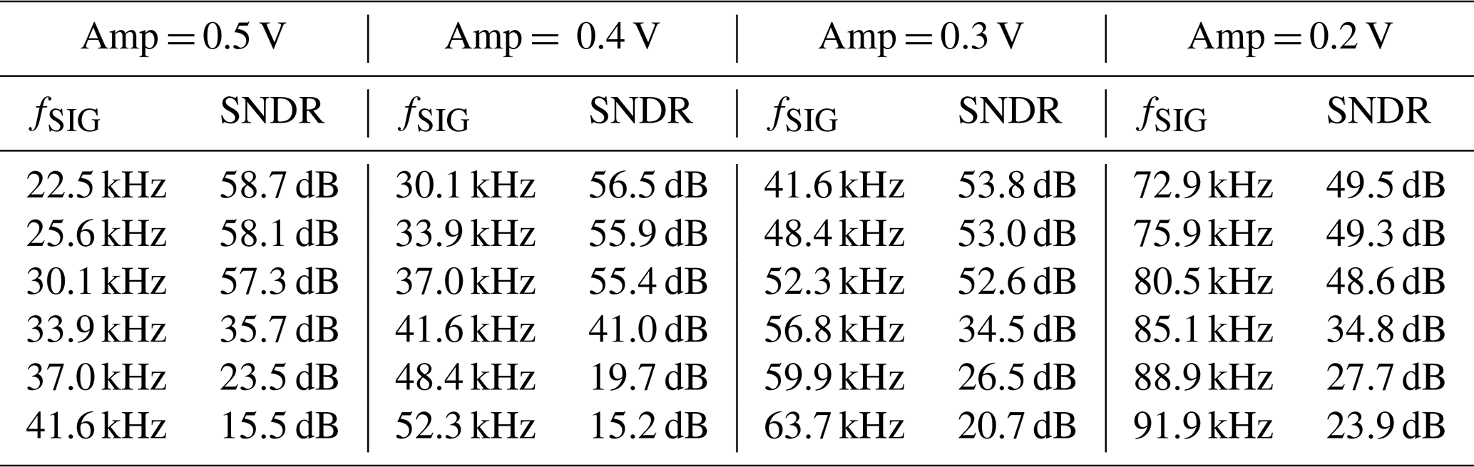

Figure 12Monte Carlo simulation of the DNL from the DAC (VLSB=1 mV), slope is from −512 to +512 mV from 1 to 82 µs.
To ensure the functionality of the ADC, Monte Carlo simulations of the DAC were undertaken, and are presented in Fig. 12. The DNL for a counting up rail to rail cycle is captured. The clock frequency is reduced to 12.5 MHz. There are gain errors, yet the DNL is less 1 LSB.
The benefit of a tracking ADC with variable step size depends on the application where the ADC is to be used. Therefore an application where a car battery voltage is measured during cranking is here discussed. The tracking ADC principle is compared through a system level simulation using Matlab-Simulink. The input signal is a voltage captured during the start-up of an engine (Fig. 13). The resolution is 16-bit and the time steps are 10 ms. The data is available in the Supplement. In Fig. 13 this signal is converted with an ideal ADC, an ADC according a proposal of Huang (2013a), which is extended to 10-bit, and the proposed 10-bit ADC. A closeup of the voltage peak is depicted in Fig. 14. The ideal ADC has a clock frequency of fideal = 2 kHz, ADC of Huang (2013a) has fHuang = 25 kHz and the proposed ADC of f10 bit = 25 kHz. The LSB voltage is VLSB = 16 mV.
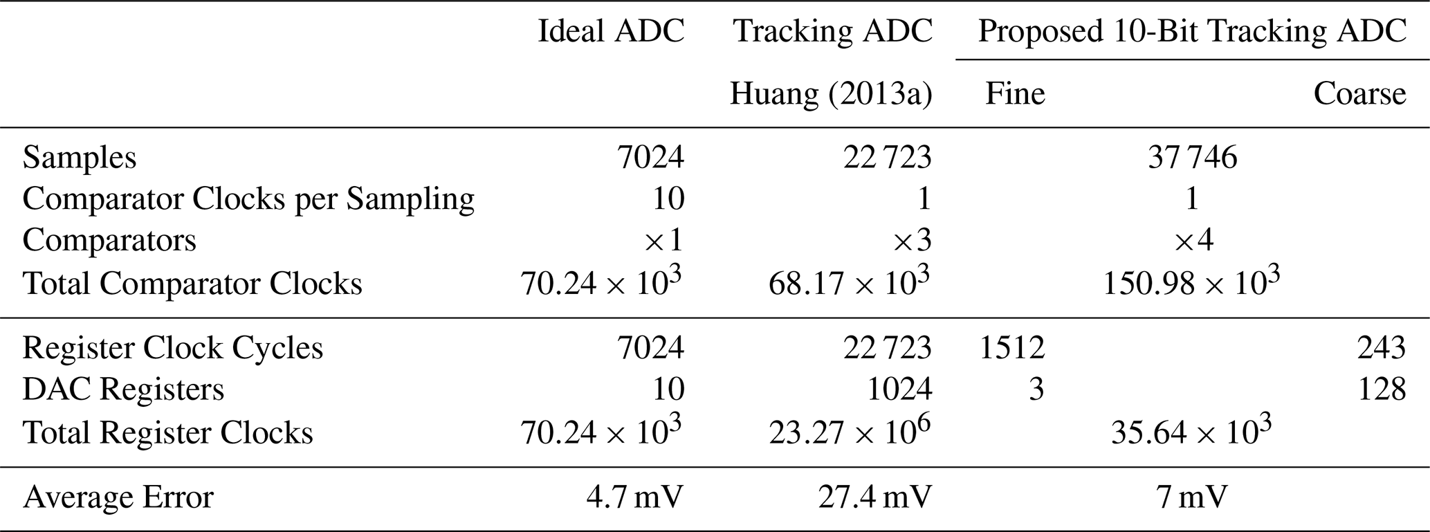
In Table 3 a summary of conversion, comparator and register clocks as well as accuracy is provided. The ideal ADC and the ADC of Huang (2013a) have a similar number of comparator clocks. The proposed ADC has twice as much comparator clocks due to its constant clock rate and because it has the largest number of comparators. According to the register clocks Huang (2013a) has the most clocks by a large margin, due to the high clock rate, the lack of ripple reduction and the large amount of thermometer coded registers. In comparison, the proposed ADC requires only 7 % of clock cycles and 0.2 % of total register clocks. The ideal ADC has nearly twice as many register clocks as the proposed ADC. The average error is calculated in the signal range from 0.9 to 2.8 s. The ideal ADC yields the best results and the proposed ADC is slightly better than Huang (2013a).
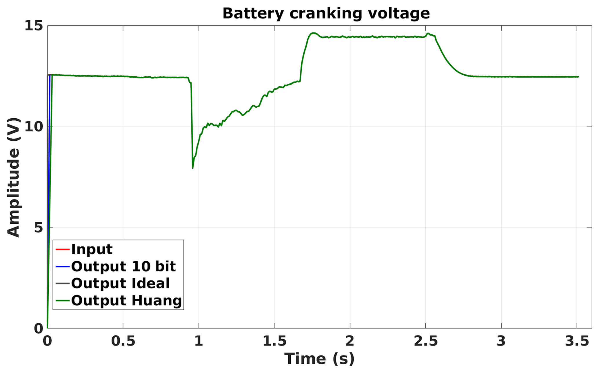

Table 3Results of ADCs for converting the test signal and the average error.
This paper presents the design and simulation of a 10-bit tracking ADC with a multi-bit quantiser and a segmented current-steering DAC. The variable step size improves the limited slew rate by a factor of 2 if clock rate is held constant. The step size is controlled by the quantiser depending on the transient of the input signal.
A further advantage is the removal of the output signal ripple. This also reduces the clocking and hence the DAC´s registers' energy consumption for low frequency input signals.
The tracking ADC presented here runs on a constant clock rate. Even if we consider an SAR used as an ideal ADC with 10 comparator cycles per conversion, our ADC exceeds the total number of comparator clocks due to sample rate and the number of comparators. According to Huang (2013a), a similar step would be a combination of variable clock sizes and variable step size. Compared to the tracking ADC of Huang (2013a) our tracking ADC improves the register's product of the DAC´s thermometer coded register chain and register clocks by nearly 4 decades. This makes a tracking ADC with 10-bit resolution reasonable at all.
The source data of cranking signal in Fig. 13 is available in the Supplement. The Matlab models may be obtained by the authors subject to confidentiality.
The supplement related to this article is available online at: https://doi.org/10.5194/ars-17-161-2019-supplement.
SB developed the Matlab models, designed the circuit and draw the IC layout. He prepared the original draft of this article. DK aquired funding by DFG, contributed to the concept, and contributed to review and editing this article.
The authors declare that they have no conflict of interest.
This article is part of the special issue “Kleinheubacher Berichte 2018”. It is a result of the Kleinheubacher Tagung 2018, Miltenberg, Germany, 24–26 September 2018.
The authors thank the German Research Community (DFG) for funding the project under grant number 250702138.
This research has been supported by the German Research Community (DFG) (grant no. 250702138).
This paper was edited by Jens Anders and reviewed by two anonymous referees.
Huang, Y., Schleifer, H., and Killat, D.: A current mode 6-bit self-clocked tracking ADC with adaptive clock frequency for DC-DC converters, 2013 IEEE International Symposium on Circuits and Systems (ISCAS2013), 2013a. a, b, c, d, e, f, g, h, i
Huang, Y., Schleifer, H., and Killat, D.: Design and analysis of novel dynamic latched comparator with reduced kickback noise for high-speed ADCs, 2013 European Conference on Circuit Theory and Design (ECCTD), 1–4, 2013b. a
Kanzian, M., Gietler, H., Unterrieder, C., Agostinelli, M., Lunglmayr, M., and Huemer, M.: Low-Complexity State-Space-Based System Identification and Controller Auto-Tuning Method for Multi-Phase DC-DC Converters, 2018 International Power Electronics Conference (IPEC), Niigata, 3140–3141, 2018. a
McDonnell, S. M., Patel, V. J., Duncan, L., Dupaix, B., and Khalil, W.: Compensation and Calibration Techniques for Current-Steering DACs, IEEE Circ. Syst. Mag., 17, 4–26, 2017, a
Moody, T., Ren, S., and Ewing, R.: 10 bit current steering DAC in 90 nm technology, NAECON 2014 IEEE National Aerospace and Electronics Conference, Dayton, OH, 337–341, 2014. a
Nazari, M., Sharifi, L., Aghajani, A., and Hashemipour, O.: A 12-bit high performance current-steering DAC using a new binary to thermometer decoder, 2016 4th Iranian Conference on Electrical Engineering (ICEE), Shiraz, 1919–1924, 2016. a
Radulov, G. L., Quinn, P. J., van Beek, P. C. W., Hegt, J. A., and van Roermund, A. H. M.: A binary-to-thermometer decoder with built-in redundancy for improved DAC yield, 2006 IEEE International Symposium on Circuits and Systems, Island of Kos, 4 pp., 2006. a
Shaker, M. O. and Bayoumi, M. A.: A 6-bit 130 MS/s low-power tracking ADC in 90 nm CMOS, 53rd IEEE International Midwest Symposium on Circuits and Systems, Seattle, WA, 304–307, 2010. a