 | 10 Dec 2020
Radar system with dedicated planar traveling wave antennas for elderly people monitoring
Sassan Schäfer
Simon Müller
Daniel Schmiech
Andreas R. Diewald
Radar systems for contactless vital sign monitoring are well known and an actual object of research. These radar-based sensors could be used for monitoring of elderly people in their homes but also for detecting the activity of prisoners and to control electrical devices (light, audio, etc.) in smart living environments. Mostly these sensors are foreseen to be mounted on the ceiling in the middle of a room. In retirement homes the rooms are mostly rectangular and of standardized size. Furniture like beds and seating are found at the borders or the corners of the room. As the propagation path from the center of the room ceiling to the borders and corners of a room is 1.4 and 1.7 time longer the power reflected by people located there is 6 or even 10 dB lower than if located in the center of the room. Furthermore classical antennas in microstrip technology are strengthening radiation in broadside direction. Radar systems with only one single planar antenna must be mounted horizontally aligned when measuring in all directions. Thus an antenna pattern which is increasing radiation in the room corners and borders for compensation of free space loss is needed. In this contribution a specification of classical room sizes in retirement homes are given. A method for shaping the antenna gain in the E-plane by an one-dimensional series-fed traveling wave patch array and in the H-plane by an antenna feeding network for improvement of people detection in the room borders and corners is presented for a 24 GHz digital beamforming (DBF) radar system. The feeding network is a parallel-fed power divider for microstrip patch antennas at 24 GHz. Both approaches are explained in theory. The design parameters and the layout of the antennas are given. The simulation of the antenna arrays are executed with CST MWS. Simulations and measurements of the proposed antennas are compared to each other. Both antennas are used for the transmit and the receive channel either. The sensor topology of the radar system is explained. Furthermore the measurement results of the protoype are presented and discussed.
- Article
(6844 KB) - Full-text XML
- BibTeX
- EndNote


Because of the rising amount of elderly people in retirement homes and the non-continuous observation by caretakers, the early recognition of emergencies should be improved further. To ensure a normal everyday life for these people a conventional vital sign monitor can not be used. The goal is to achieve a non-invasive alternative with a planar microstrip patch antenna based radar system which can monitor people's vital signs while they move freely around in their home. There have been many activities in microwave-based vital sign monitoring in the last decade as active radar MMICs become less expensive. Radar is a breaking technology for vital sign monitoring because microwaves are invisible and can penetrate through dry clothing and walls. Many activities are based on standard radar systems (classical CW or FMCW systems) with conventional antenna designs and by optimizing the signal processing (Will et al., 2015). Signal processing in the time domain based on matched filters, auto-correlation or cross-correlation with sample functions is preferred. A very good overview about vital sign radar activities for different applications like elderly people monitoring, children monitoring (against sudden infant death syndrome) or driver's health monitoring is summarized in Will et al. (2017).
In two former conference contributions the authors have shown in detail the concept of the antenna design for monitoring elderly people in retirement homes (Schäfer et al., 2018a, b).
The authors tried to optimize the technological prerequisite in order to improve the subsequent signal processing. Thus a digital beamforming system with 2 TX and 4 RX-channels will be applied. The technological setup has already been outlined in Schäfer et al. (2019). In this work the antenna design and the technological setup are combined to a prototype system. Preliminary measurements are done and presented in this paper.
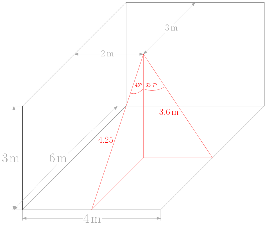
The system is designed for installation on the ceiling of a standard room in a retirement home, the location is in the middle of the room. This average size is determined for a conventional room in a retirement home by 3 m in height, 4 m in length and 6 m in width as outlined in Fig. 1. Due to higher distance from the radar system to the corner of the room, than right to the floor below, a standard patch array is unsuitable. In order to illuminate the rooms perfectly dedicated antenna arrays with a heart-shaped antenna pattern in the E- and the H-plane are developed.
A microstrip patch antenna line array (LA) is used for compensation by increasing the radiation power in the E-plane direction. In Sect. 2 the antenna specification is described and in Sect. 3 a solution for pattern design in the E-plane due to a line array (LA) is given. The design of the proposed antenna and simulation with CST MICROWAVE STUDIO (CST, 2020) in the K-band at a frequency of 24 GHz are shown. The comparison of measurement and simulation is given.
The radiation compensation needs to be solved in the H-plane, too. A parallel feeding network (PFN) for the individual line arrays is designed in order to compensate the gain in the H-plane. In Sect. 4 the transmission characteristics and the feeding network design will be described and the microstrip patch antennas are shown.
In Sect. 5 the sensor set-up and the layout is described. Measurement results of the complete prototype system will be shown. The influence of the antenna farfield is discussed. Section 6 concludes this paper.
The average room size in retirement homes is supposed to be 3 m in height, 6 m in length and 4 m in width as outlined in Fig. 1. These dimensions are taken from an exemplary room in a retirement homes of the cooperative project partner. Of course, these dimensions will vary between different retirement homes slightly, the general concept of radiation enforcement in non-broadside direction is essential for “ceiling-to-bottom-looking” radar systems. Objects in the room which are not shadowing people to be monitored are later on cancelled out by the signal processing due to their static behaviour.
In order to monitor the complete floor area a triangle with a base of 4 m and the height of 3 m is assumed for the radiation pattern. As the sensor will be installed in the middle of the roof the triangle is symmetric. Thus a opening angle for the antenna would be . The distance from the sensor to the floor (direction defined as and ) is 3 m, from sensor to the floor-wall corner ( and ) is 3.6 m. Analyzing the radar equation
shows that for targets with constant radar target cross section σ the receive power at a radar with isotropic antenna pattern () is more than factor 1∕2 lower when located in the corner instead of to be located directly below the sensor. In addition patch antennas radiate their maximum of power in the broadside direction (, ) thus the receive power of targets below the sensor is much higher compared to targets in the corner. As the radiation pattern of the receive antenna is multiplied with the pattern of the transmit antenna it is sufficient to modify only one antenna in order to compensate the power reduction due to angle and distance, at least for one plane, E-plane or H-plane.
The free-space loss due to higher distance at is 4dB, the power reduction of a standard patch antenna under for the transmit antenna is approx. 3-4dB. Thus the receiving line-array needs to have an approx. 10dB higher gain in compared to broadside direction.
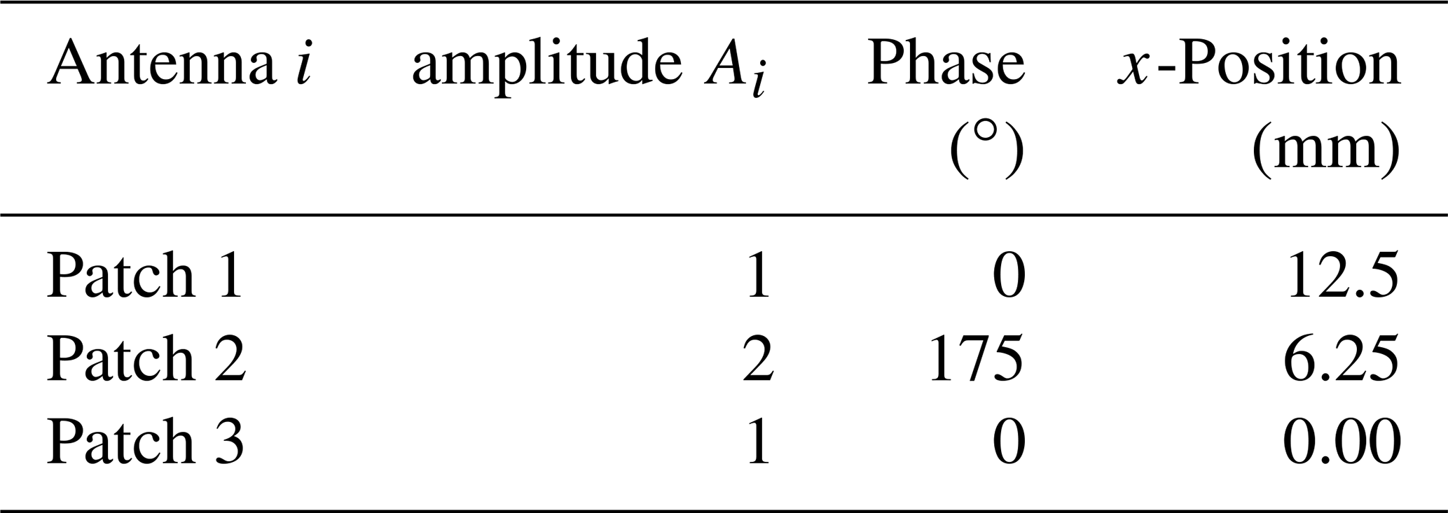
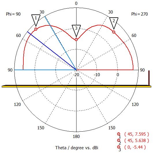
For this the amplitude and phase of single patches with distance of λ∕2 need to be found which can easily be done with the farfield array toolbox of CST MICROWAVE STUDIO. Here a superposition of three times a standard patch shifted in space and phase and with adjusted amplitudes are calculated.
In the actual prototype a radar MMIC is used which has 2 transmit channels and 4 receive channels (only I-signals), the latter are used for a digital beamforming application in the H-plane. Thus the spacing between the antenna is only and only one-dimensional line-arrays are possible. This allows beamshaping in the E-plane which will compensate the radiation pattern of the transmit antenna with parallel feeding network (PFN, in next section) which will be a standard patch array with beamshaping in the H-plane.
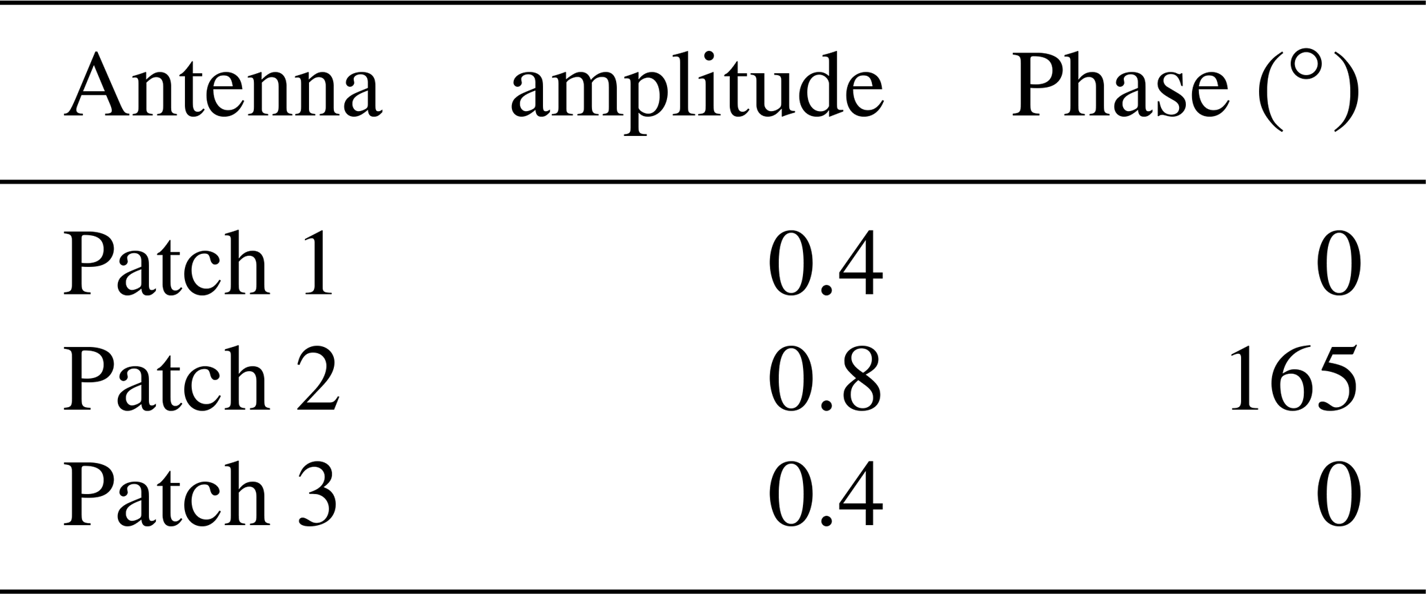
The parameters which fulfill the antenna specification in the section before are given in Table 1, the superposition of radiation pattern corresponding to the table are found in Fig. 2.
Table 1Phase and amplitudes of patch antennas to fulfill the specification.
The complete line array will consist of three microstrip patch resonators which are series-fed with microstrip lines. The last patch would be a single-port standard patch. The patches are optimized in radiation for 24.125 GHz, the center of the 24 GHz ISM band. The substrate is a RO4835 material with a design permittivity ϵr=3.72. The microstrip line width for a 50Ω transmission line is wt=0.507 mm. The first two patches are two-port patches for which the design parameters need to be determined.
3.1 Design of Microstrip Patches
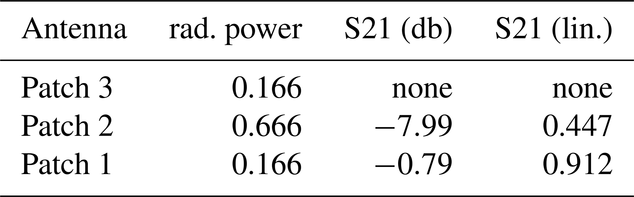
Each single patch is designed for low reflection with Γ≈0 at the feeding port (port 1). In the following the balance between radiated power and transmitted power to port 2 is adjusted. The last patch (i=3) with power absorption of 100 % is already finished. The amplitude of the second patch (i=2) is twice the amplitude of the last patch which yield a four times higher power. Thus the second patch needs to accept the power which is radiated by itself and the power which is transmit to the last antenna. The radiated power of antenna k is given with
The transmission coefficient S21 is given with
Table 2 shows the transmission coefficients which should be adapted to the given amplitudes. The phase of the coefficient will be adjusted later by conventional delay lines.
Table 2Radiated power and transmission coefficient S21 of each patch.
The adjustment of the recess length l1 at the input port has the most effect on the input reflection. The patch width wp but also the recess length l2 and recess width w2 at the output port are influencing the transmission coefficient S21. Thus the reflection and the transmission can mostly be controlled independently. The input reflection of each patch is lower than 12dB in the complete ISM band. The dimensions and the patch design are given in Fig. 3.
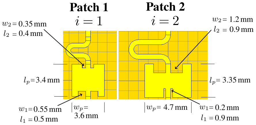

The first patch (i=1) reaches a reflection of dB and the middle patch (i=2) dB at the center frequency of the ISM band (24.125 GHz). The resulting transmission parameters are shown in Fig. 4 with linear scale for better understanding (all further S-Parameters are given in logarithmic scale). The first patch achieves a transmission of S21=0.89 and the middle patch of S21=0.46 in the relevant frequency range. Compared with Table 2, these values are close to the specifications.
3.2 Feeding design
The spacing between the patches is λ∕2 which equals 6.25 mm. The length of the patches is around lp=3.167 mm up to 3.4 mm. Due to the different patch lengths variable spacings appear between the patches. There is a space of 2.838 mm between patch 1 to patch 2 and of 2.9708 mm between patch 2 to patch 3. This space is used for phase adjustment of the several patches. The phase difference corresponding to the specification in Table 1 is defined from the reference plane of the first patch which is the patch edge at the ending of the recess to the comparable reference planes of the subsequent patches. The feeding microstrip lines are designed as short as possible in order to reduce the losses. The design of the feeding lines is shown in Fig. 3, too.
3.3 Antenna simulation
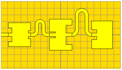
In Fig. 5 the completed one-dimensional antenna line array is shown. The total antenna length is l=15.694 mm and the maximum width is w=6.3389 mm. In Fig. 6 the antenna reflection coefficent is shown by simulation.
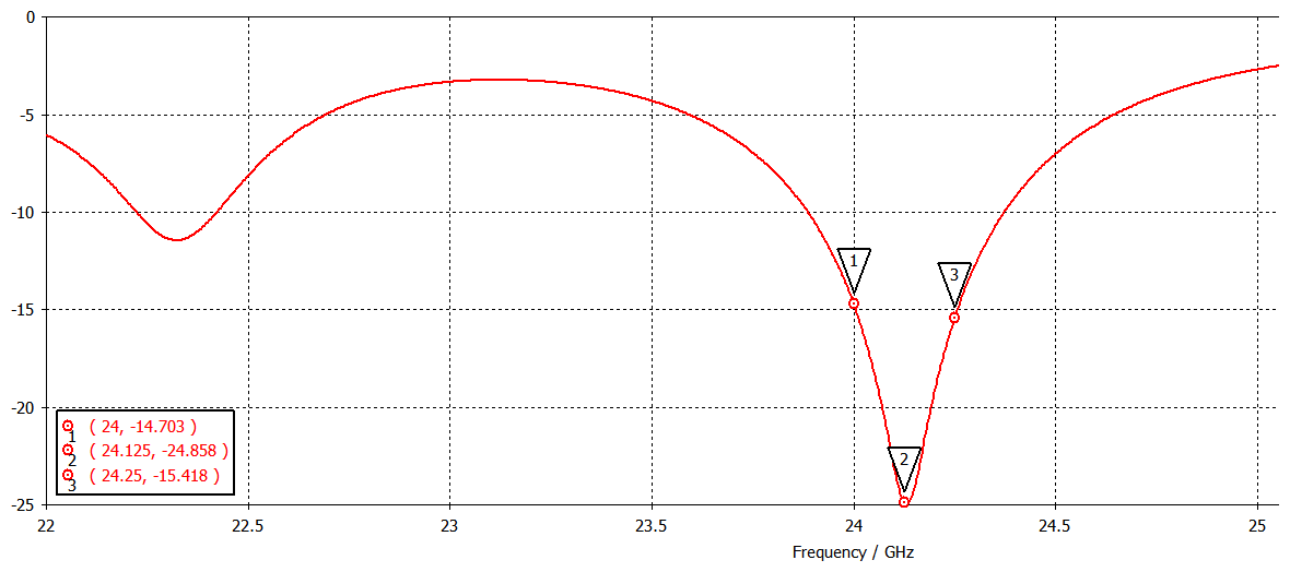
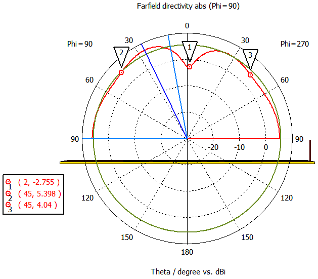
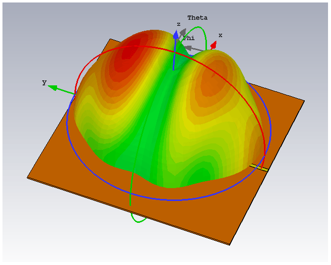
A reflection of less than −15 dB is obtained in the 24 GHz ISM band and the minimal reflection of −24.85 dB is reached at the center frequency of 24.125 GHz. For this antenna design a sensitivity analysis has not been done separately, a general analysis of production tolerances in the EUROCIRCUIT manufacturing process has been executed by the authors in Müller et al. (2016a). It is assumed that the deviations in resonance frequency and amplitude in the presented antenna design will be comparable to those in Müller et al. (2016a). The farfield in the E-plane yields a satisfying pattern with a gain difference of 8 dB at 0∘ compared to 33.7∘ which is shown in Fig. 7. Due to the microstrip feeding of the single patches the radiation of the single patches is not symmetric and the radiation pattern is squinted. Thus a symmetric pattern of the line array is not achieved. The total 3D antenna farfield pattern is shown in Fig. 8.
3.4 Measurement
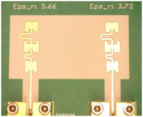
The line array antenna was developed for a design permittivity of 3.66 which is given as number in the datasheet of ROGERS at 10 GHz and for a permittivity of 3.72 which could be taken from a measurement graph in the datasheet. Both antennas have been processed at the EUROCIRCUITS process which has been investigated for RF designs in Müller et al. (2016a, b). The photo is shown in Fig. 9 which is later in the manuscript. The antennas are connected to a matched connector described in Diewald et al. (2017).
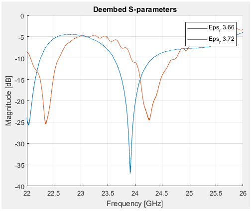
The antennas are measured with a Rohde&Schwarz ZNB40 network analyzer and the connectors are deembed with the method explained in Müller and Diewald (2015). The reflection coefficient is shown in Fig. 10.
The antenna pattern in the E-plane is measured again with the Rohde&Schwarz ZNB40 and a horn antenna ARRA 42-862 with an operation range from 18 up to 26,5 GHz in the anechoic chamber of Trier University of Applied Sciences.
The results and the comparison with the farfield simulation is depicted in Fig. 11. The S-Parameters of the antenna designed with a relative permittivity of εr=3.72 are fitting very well for the reflection coefficient. The complete 24 GHz ISM band is covered with a maximum reflection coefficient of dB. Also the antenna design for εr=3.66 is below dB for the complete ISM band, but the fit with the simulation is not good. This shows, that for CST MWS simulation (without the new roughness modell) of patch antennas in the 24 GHz ISM band a permittivity of εr=3.72 should be used. In addition the fit between the simulated and measured farfield results are sufficient but should be optimized in a further design review. Especially at broadside direction an additional beam is occuring which is assumed to be caused by surface wave edge effects of the PCB. Nevertheless the antenna characteristics meet the antenna specification.
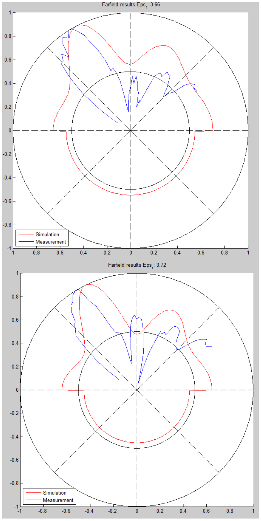
Figure 11Comparison of simulation and measurement results of the farfield in the E-plane for both antennas.
The radiation compensation needs to be solved in the H-Plane, too. A parallel feeding network for the individual line arrays is designed in order to compensate the gain in the H-plane. In the following the parallel feeding network (PFN) connection to microstrip patch antennas is shown. The parallel fed patches transmitted power and phase can be determined as similar as for the line arrays. Deduced from the specified room size a radiation angle of is required. In this case the radiation pattern of a single patch antenna which has been simulated before is superposed for three patches adjacent to each other (in H-plane dir.) with a distance of λ∕2.
The resulting specifications are shown in Table 3. The related farfield radiation in the H-plane is shown in Fig. 12.
Table 3Phase and amplitudes of patch antennas to fulfill the specification.

The required radiation difference between the broadside direction () and the corner direction () is 12 dB
4.1 Three-step Microstrip Power Divider
Based on the specifications in Table 3 a three-step power divider needs to be build. This power divider has to divide the input power in three branches which run parallel in a distance of mm. The center branch guides a wave whose power is four times higher than the outer branches and requires a phaseshift of 165∘.
Due to the high power difference in the branches a direct power division can not easily be realised because the required input impedances would have extreme values (e.g. 160Ω which is higher than the maximum realisable microstrip impedance of 80Ω). Thus the idea is to split the power division in three steps. This idea enables the possibility to realise high power differences with high precision at the output ports. For these two Wilkinson Power Dividers and one combiner are used. To reduce the reflection loss, quarter wavelength transformers are used to match the 50Ω signal line. Both, power divider and transformer, are described in Pozar (2011). In total four dividers are needed which are simulated separately to achieve higher accuracy. By reason of the simulation results of Schäfer et al. (2018a) a relative design permittivity of ϵr=3.72 is used.
The first used divider needs to seperate the input power in two identic signals with half of the power. Thus, to achieve a power ratio of 1 : 1, both branch impedances have to be two times higher than the divider input impedance. A divider input impedance of 25Ω is chosen, so the branch impedances is the standard 50Ω signal line. The microstrip width is approximated by the formulas described in Pozar (2011) and exactly determined in use of CST MICROWAVE STUDIO. In Fig. 13 the first divider layout is shown on the left side. The simulated transmission coefficient in both branches amounts to −3.6 dB.
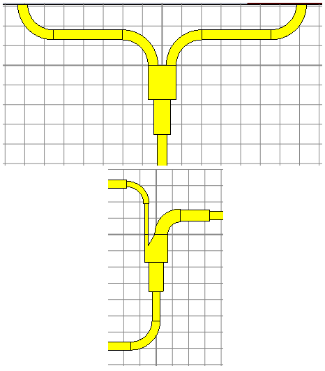
Figure 13First Power Divider with ratio 1 : 1 (left side) and second Power Divider with ratio 2 : 1 (right side).
Both branches are guided next in a divider with a power ratio of 2 : 1. So the previous split power is now divided to 1∕3 and 2∕3. Thus the impedance value in the left branch is three times higher, in the right branch 3∕2 times higher than the divider input impedance. Due to the EUROCIRCUITS manufacturing process, the microstrip width is limited at least at 100 µm. The maximum impedance at ROGERS RO4835is 90Ω. Because of the already determined impedances in the previous power divider, the divider input impedance is set to 25Ω. The branch impedances result in 75Ω and 37.5Ω. In Fig. 13 the second divider is shown on the right side. In the upper left branch a transmission of −5.6 dB and in the right of −2.16 dB at 24.125 GHz is achieved by simulation, thus a power ratio of 2.2 : 1 results. By use of a recess slot in the branch the transmission characteristic can be adjusted.
Two of the resulting microstrip lines conduct 1∕6 and two further lines conduct 1∕3 of the input power. Combining the two latter microstrip lines which conduct 1∕3 of the input power will yield a four times higher transmit power than the two outer branches. Because both of these branches guide the same mode, the previous designed 1 : 1 power divider can be reversed as power combiner. Due to symmetric excitation on the two input ports the resistance which is typical for Wilkinson Dividers could be neglected. Power combining both branches yields a simulated transmission of dB.
4.2 Complete Parallel Feeding Network
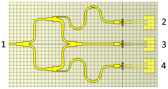
After simulating the dividers in a segmented approach, the dividers and the combiner are merged to a final layout. The resulting Parallel Feeding Network (PFN) has a total length of 28.334 mm and width of 15.57 mm and is shown in Fig. 14.

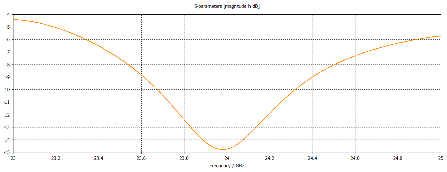
The return loss minimum is located outside of the 24 GHz ISM band at 24.9 GHz at −33 dB, however a return loss of −24.7 dB at 24.125 GHz is achieved which is given in Fig. 15.
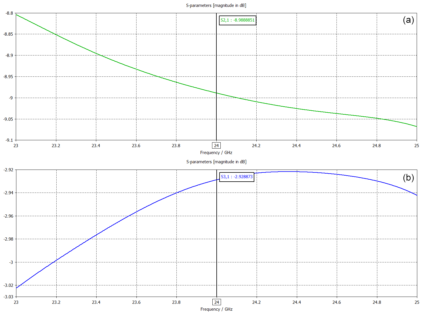
The two outer branches are extended with additionally microstrip lines in order to reach the phaseshift difference of 165∘ to the inner branch. In the outer branches (port 2 and 4 in Fig. 14) a transmission of −8.98 dB and the inner branch (port 3 in Fig. 14) a transmission of −2.92 dB is achieved in the simulation thus a total power difference of 4.017 : 1 is attained as it is shown in Fig. 16 for both ports.
By reason of the feeding network radiation, mainly in the E-Plane, which interferes with the radiation pattern of the patch antennas, the feeding network and the patch antennas are separated on top and bottom layer. Since the sensor prototype is built on a 4-layer PCB, the test antennas are designed likewise. To conduct the signal to another layer, the microstrip line vias designed in Schmiech et al. (2018) are used. First, a test antenna with the PFN and single patches is simulated which is outlined in Fig. 14. Thus the radiation pattern in the H-plane and accuracy of the parallel feeding can be evaluated. The simulated antenna reflection coefficient is depicted in Fig. 17.
In the whole 24 GHz ISM band a reflection lower than dB is accomplished. Due to the feeding network there is also radiation on the backside of the PCB which is depicted in Fig. 18. According to simulation a gain difference of about −20 dB results.
4.3 Measurements
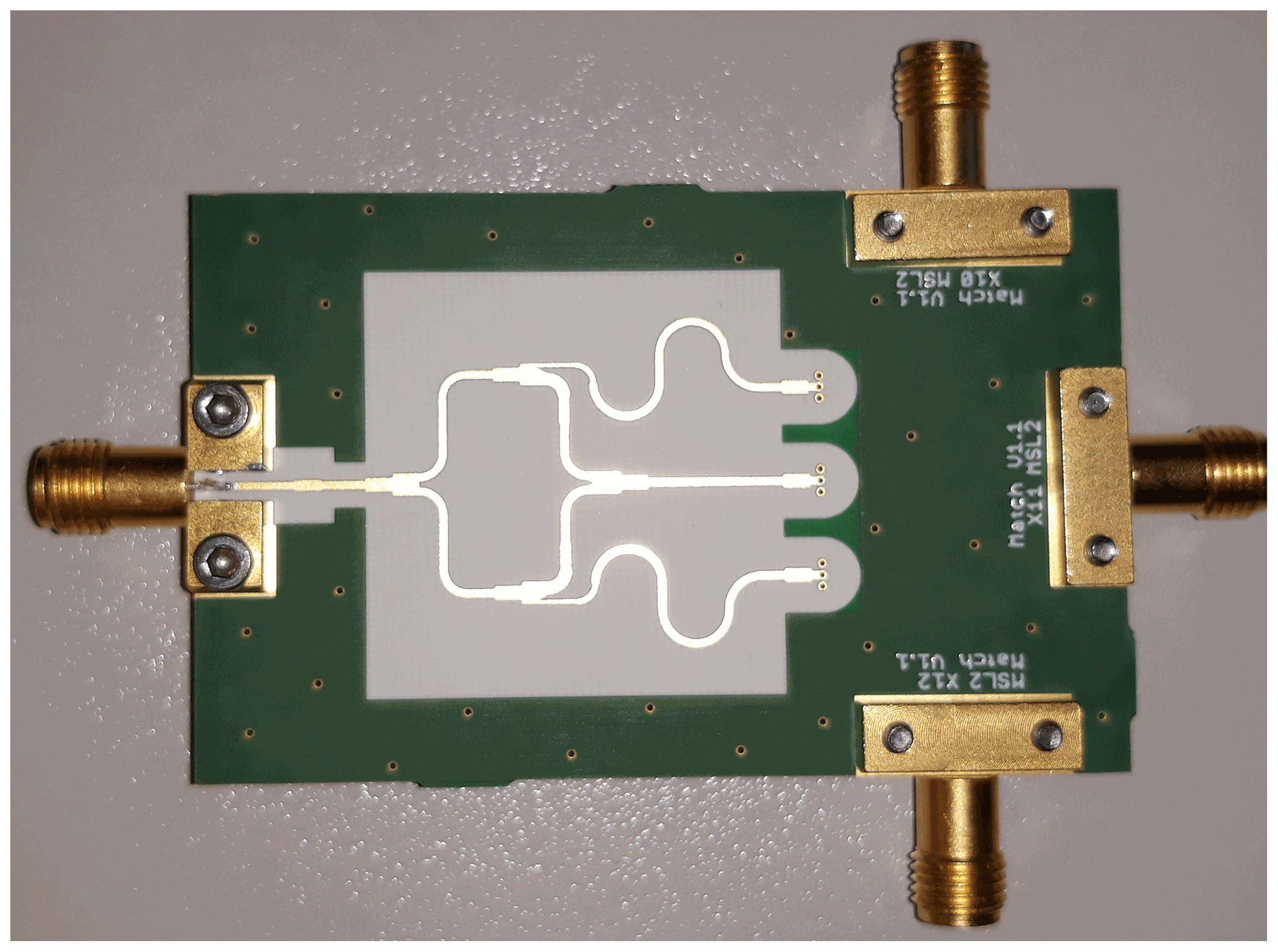
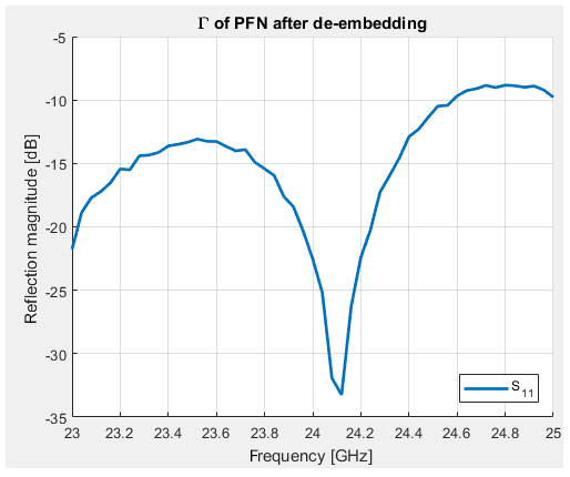
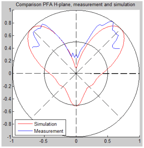
First, the feeding network is manufactured (Fig. 19) on a Rogers RO4835 (10 mil) substrate and measured with a Rohde&Schwarz ZNB40 network analyzer. A reflection minimum of dB at the center frequency of 24.125 GHz is obtained in Fig. 20. The transmission coefficients of all three branches result in a transmission difference of factor 3.86, with a transmission of −6.35 dB in the middle branch and a transmission of −12.2 dB at the center frequency.
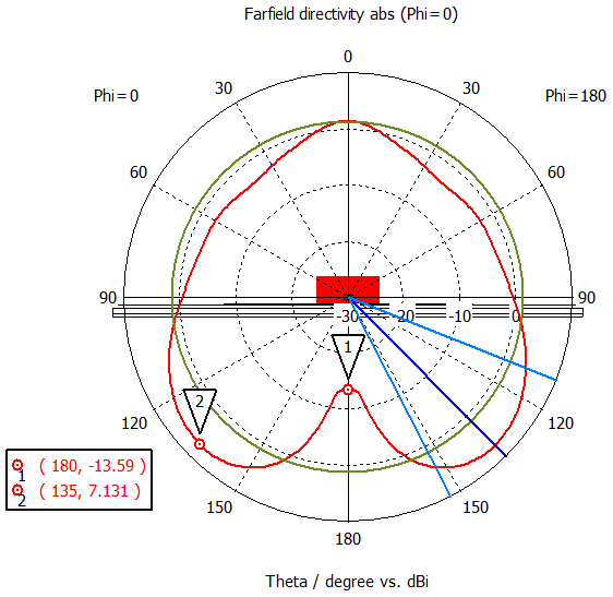
The measured radiation pattern (realized gain) of the PFN including patch antennas on a second PCB is plotted linearly and compared to the simulation in Fig. 21. The gain difference of to is 11 dB which matches the specification.
In previous sections the authors presented dedicated microstrip patch arrays. The first antenna is an one-dimensional series-fed traveling wave antenna with a heart-shaped antenna pattern in the E-plane, while the second antenna is parallel-fed and has heart-shaped pattern in the H-plane.
5.1 Sensor Setup
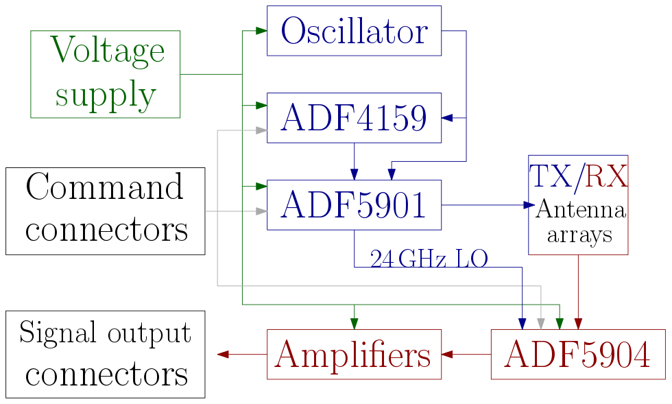
In terms of cost and time reduction in the development, the baseband electronics, signal and voltage supply connectors are taken over from a laboratory radar already implemented in our institution (Dirksmeyer et al., 2018). Thus the PCB outline and the connector placement for the RF front-end is equal to the laboratory radar. The transmitting part is implemented with an ADF4159 waveform-generator and an ADF5901 VCO and LO which is used for signal generation. As reference clock a 100 MHz oscillator is utilised. The receiving part is set-up with an ADF5904 four channel receiver. The differential signals, which are received and down-converted, are connected to an AD8422 instrumentation amplifier with single ended outputs. Both kinds of signals are provided for signal processing, the differential signals without gain and the single ended signals with a gain of 200. For further information about applications of the on-board ICs, the datasheets are highly recommended. The circuit board manufacturing process for RF PCBs by EUROCIRCUITS has been investigated in Müller et al. (2016a, b).
5.2 RF-Frontend Layout
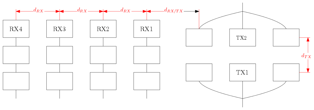
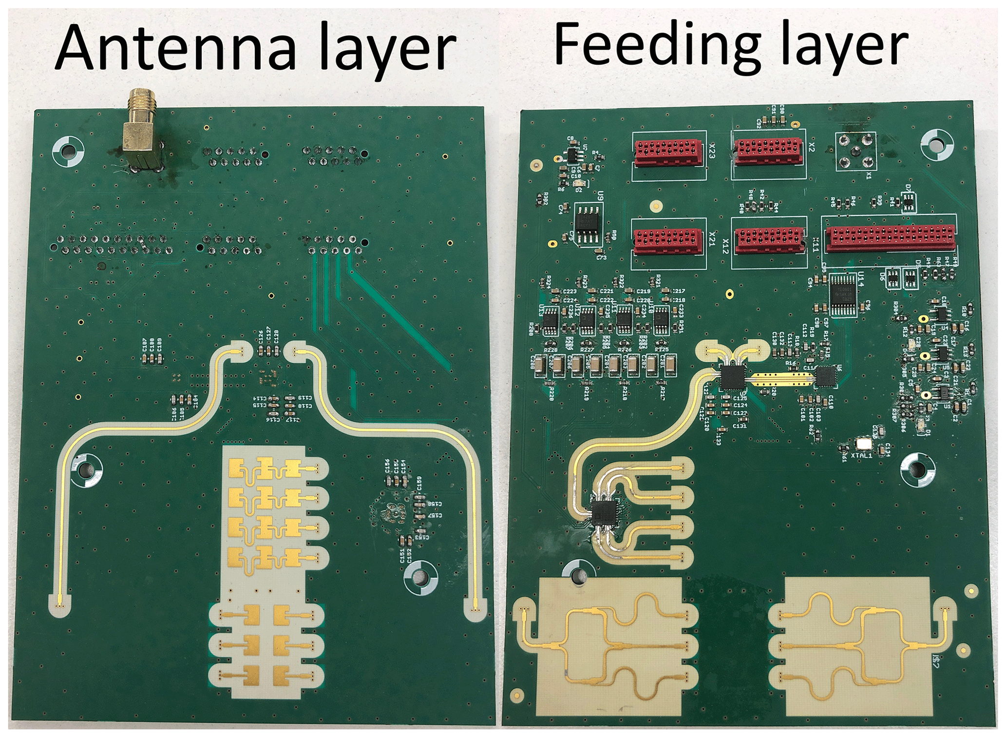
Unlike the electronic components, the transmitting and receiving antennas are located on the PCB downside. The two transmitting and the four receiving antennas are placed with a spacing of half wavelength of mm to the adjacent antenna. In consideration of the high space usage of the feeding network, the parallel fed patch array of Sect. 4 is used as transmit antennas. The one-dimensional series-fed microstrip patch arrays of Sect. 3 are used as receive antennas. To reduce the coupling between transmit and receive antennas on board, the spacing between the two different arrays is determined to dRX/TX=11 mm. The schematical layout and an overview about the spacings is given in Figs. 22 and 23. Due to the λ∕2 spacing of the receive antennas a distinct angle determination is achieved in the H-plane by digital beamforming (DBF) processing. By switching the power between the two transmit antennas a 2.5D MIMO radar imaging is applied. The angle-of-arrival (AoA) in the E-plane could be measured. Figure 24 shows the front and the back side of the protoype PCB for testing and evaluation.
5.3 Data Acquisition
The measurement set-up of Dirksmeyer et al. (2018) will be reused as the connector placing is equal.
In this set-up National Instrument devices are used:
-
The docking station cDAQ9174
-
The NI9402, a digital input/output module which is used to generate the ramp trigger signal
-
The NI9220, an analog input module to provide the data for further signal processing
The measurement is done in the 24 GHz ISM Band. The radar operates works in FMCW mode and is triggered for a ramp repetition frequency of 390 ramps per second. The sampling rate of the NI9220 is 100 000 samples per second which results in 256 samples per ramp.
5.4 Data Processing
The measurement is done in a low reflection absorber chamber in the basement of our institution at the Trier, University of Applied Sciences. The remaining effects can mostly be removed due to a calibration measurement. The goal of the measurement is to detect a corner reflector with a radar cross section of 40 m2, in a distance of 2 m in five different angles to ensure a wide angle surveillance of the system. These are the directions in which the main radiation of the developed antennas is optimized, additionally the broadside direction as comparison measurement is done. To evaluate all five angles, the corner reflector is located in front of the radar system and the whole radar system has to be turned by a mechanical rotation system in the relevant directions as shown in Fig. 25. First the calibration measurements are done in all five directions without corner reflector. Then the empty space can be removed in the measurement afterwards. As example the processed signal of one receive antenna is shown in Fig. 26 with and without the corner reflector.
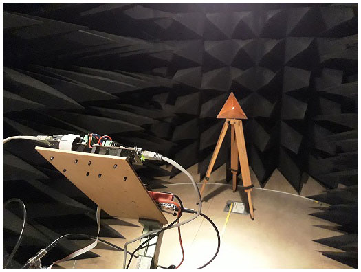
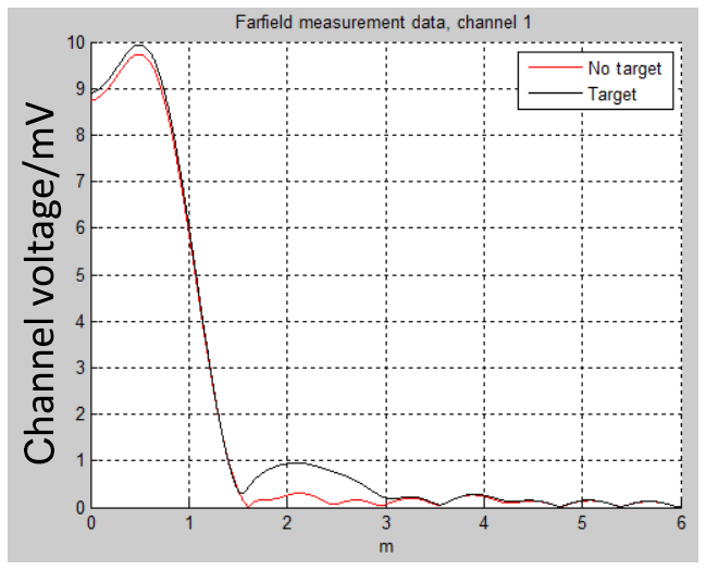
In a distance of 0.5 m a virtual target is detected in both measurements. However no target is placed in that distance, as it could be seen in the measurement setup in Fig. 25. On the one hand the corresponding “ghost target” occurs probably due to cross talk of baseband electronics which should be fixed in a layout review. On the other hand electronic offset and linear variation during the frequency ramp are enforcing this problem. The latter could by canceled by subtracting the linear regression. For the measurement this specific error is not an obstacle since it can be suppressed by taking into account the calibration which is a difference of both signals.
In both measurements the noise ratio of other interferences is reduced due to the absorber chamber, therefore the only difference could be found in a distance of 2 m which is the target's location shown in Fig. 27.
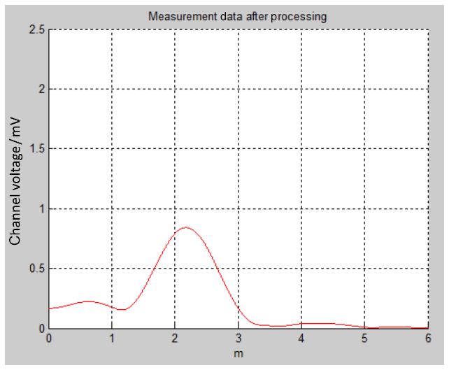
Figure 27Range data difference of channel 1 with and without a target in broadside direction.
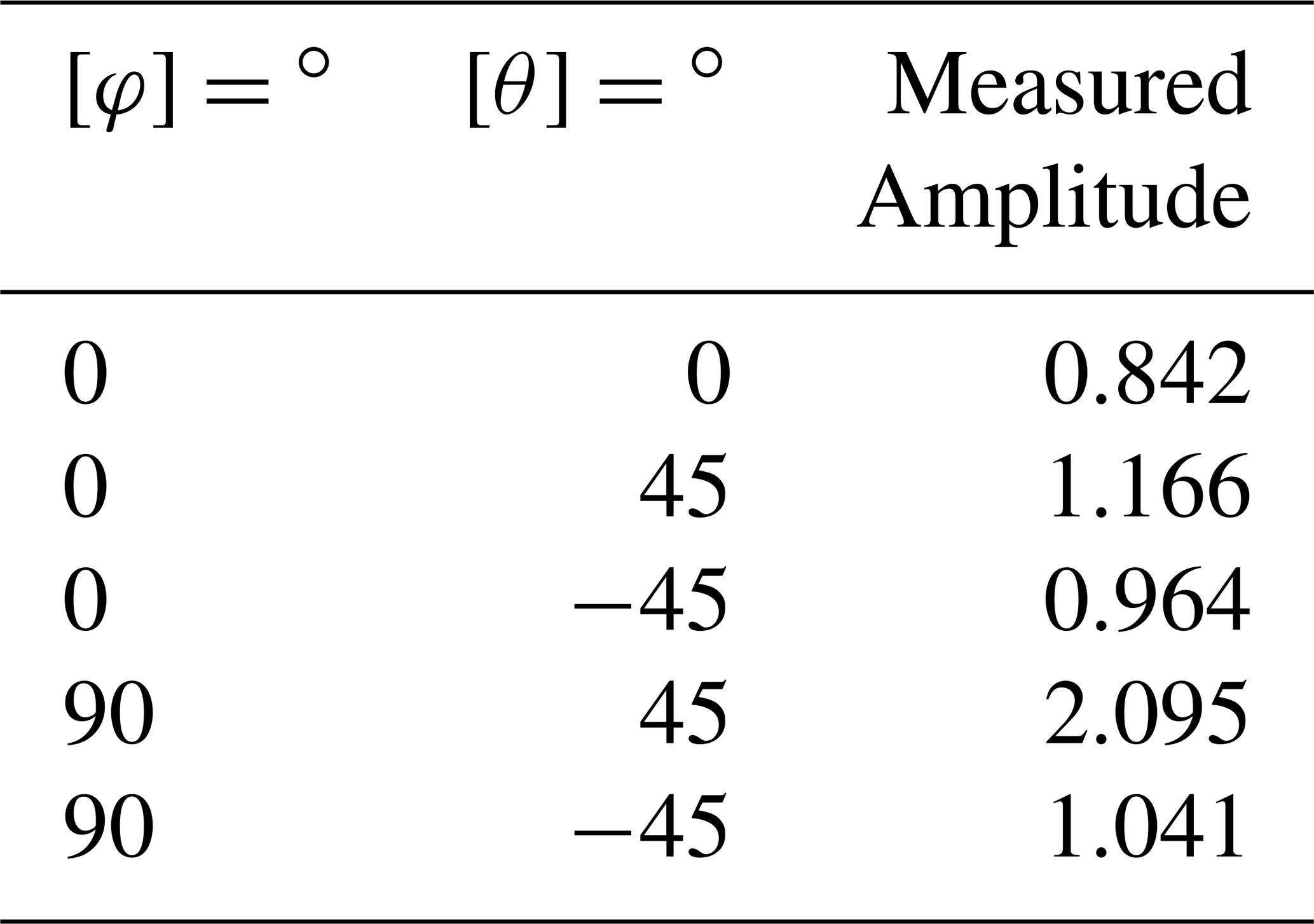
The result is satisfying, since most of the noise and side effects of the measurement are removed and the target in a distance of 2 m is seen. In Table 4 all measured angles and resulting amplitudes of channel 1 of the radar system are shown.
Furthermore the corresponding range plots of channel 1 are given in Fig. 28.
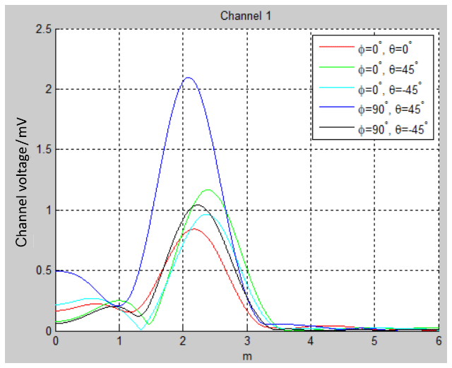
Figure 28Range data difference of channel 1 with and without a target in multiple directions.
In broadside direction, the red trace in Fig. 28, the received power is the lowest compared to each other direction, which is intended, because the system is installed in the middle of the ceiling. Thus the distance to objects directly below the sensor is lowest.
The aim for the remaining directions is to receive a signal with a comparable or even higher amplitude. The measurement results in the H-plane are expected to be the same in both directions, due to the symmetry of the parallel fed array. However the unsymmetric H-plane pattern of the line array also interferes with this direction. Thus the direction , (green trace) and , (cyan trace) do not match exactly. The reason of the H-plane mismatch is identified by the asymmetric round feeding lines between the patches.
For both measurements in the E-plane (blue trace for , and black trace for , ) the received amplitude in “forward direction” (, ) is about twice as much as in the opposite direction. This effect mainly results from the E-plane of the line array, shown in the farfields in Fig. 11 where radiation in forward direction is two times higher than in the “backward direction”. Nevertheless the difference of the ampllitudes is only 3 dB which is much lower compared to classical patch arrays.
In this paper two different antennas for ceiling suspension are developed which compensate free space losses in domestic environments and the typical radiation characteristic of standard patches. The comparison between simulation and the measurement of the antennas are promising, a wide view angle and a compensation of free space losses has been accomplished in order to cover a complete size of an average room as shown in Fig. 1. A protoype system for vital sign monitoring of elderly people has been developed. The results in all radar channels are satisfying, since a wide angle for target detection is achieved.
For further design reviews the antenna pattern of the line array in broadside direction and the match to the simulation should be optimised. The gain difference in the E-plane should be compensated and the squinting in the H-plane, maybe by use of symmetric feeding lines between the patches, could be reduced for the line array.
The parallel fed array is matching well to the simulation, but the large space requirements of the feeding is an obstacle. By finding a solution for this size problem the system dimensions could be minimized.
In the next step the prototype is evaluated for standard measurement scenarios and a signal processing software will be developed to measure the breathing rate and the heart-beat rate of people located below the sensor.
No data sets were used in this article.
SaS was working as Bachelor student at the Laboratory of Radar Technology and Optical Systems, he designed all antenna elements in CST MWS, transferred the layout to Gerber, manufactured the PCBs and measured these. SM supervised the work in the RF technology and DS supervised the work for microwave based vital sign monitoring and signal processing. ARD is the head of the institution, he gave the initial idea of the application, the design specification of the antennas, the radar system topology and the workflow to proceed the measurements.
The authors declare that they have no conflict of interest.
This article is part of the special issue “Kleinheubacher Berichte 2019”. It is a result of the Kleinheubacher Berichte 2019, Miltenberg, Germany, 23–25 September 2019.
The authors would like to thank Dieter Hewener from Senioren-Pflegeheim Holunderbusch GmbH in Lorscheid for the kind introduction into retirement homes and the support in the specification of the prototype room size.
This research has been supported by the German Federal Ministry of Education and Research (BMBF) within the public funding program “FHProfUnt” with the title “VITASENS” (grant no. 13FH303PX6).
This paper was edited by Lars Ole Fichte and reviewed by two anonymous referees.
CST Microwave Studio®: http://www.cst.com/products/cstmws, last access: 9 September 2020. a
Diewald, A. R., Müller, S., and Olk, A.: PCB-Side Matching Networks for coaxial connectors, AMTA 2017 Proceedings, Antenna Measurement Techniques Association Symposium (AMTA), 15–20 October 2017, Atlanta, GA, USA, 2017. a
Dirksmeyer, L., Diewald, A. R., Müller, S.: Eight Channel Digital beamforming Radar for Academic Lab Courses and Research, 19th International Radar Symposium, 20–22 June 2018, Bonn, Germany, 2018. a, b
Müller, S. and Diewald, A. R.: Methods of Connector S-Parameter Extraction Depending on Broadband Measurements of Symmetrical Structures, The Loughborough Antennas and Propagation Conference (LAPC) 2015, 11 November 2015, Loughborough, UK, 2015. a
Müller, S., Thull, R., Huber, M., and Diewald, A. R.: Microstrip patch antennas on EUROCIRCUITS process, 2016 Loughborough Antennas & Propagation Conference (LAPC), 14–15 November 2016, Loughborough, UK, 2016a. a, b, c, d
Müller, S., Thull, R., Huber, M., and Diewald, A. R.: Analysis on microstrip transmission line surface coatings, 2016 Loughborough Antennas & Propagation Conference (LAPC), , 14–15 November 2016, Loughborough, UK, 2016b. a, b
Pozar, D. M.: Microwave Engineering, 4th edn., 10/12, John Wiley & Sons, Inc., Hoboken, USA, 2011. a, b
Schäfer, S., Schmiech, D., Müller, S., and Diewald, A. R.: One-dimensional Patch Array for Microwave-based Vital Sign Monitoring of Elderly People, IRS 2018, International Radar Symposium 2018, 20–22 June 2018, Bonn, Germany, 2018a. a, b
Schäfer, S., Schmiech, D., Müller, S., and Diewald, A. R.: Parallel Fed Patch Array for Microwave-based Vital Sign Monitoring of Elderly People, EuMW 2018, European Microwave Week, 23–27 September 2018, Madrid, Spain, 2018b. a
Schäfer, S., Müller, S., Schmiech, D., and Diewald, A. R.: Sensor Development for Vital Sign Monitoring of Elderly People, 2019 International Conference on Electromagnetics in Advanced Applications (ICEAA), 9–13 September 2019 , Granada, Spain, 2019. a
Schmiech, D., Müller, S., and Diewald, A. R.: 4-Channel I/Q-Radar system or vital sign monitoring in a baby incubator, GeMiC 2018, German Microwave Conference, 20–22 June 2018, Freiburg, Germany, 2018. a
Will, C., Shi, K., Lurz, F., Weigel, R., and Koelpin, A.: Intelligent signal processing routine for instantaneous heart rate detection using a Six-Port microwave interferometer, 2015 International Symposium on Intelligent Signal Processing and Communication Systems (ISPACS), 9–12 November 2015, Nusa Dua, Indonesia, 483–487, 2015. a
Will, C., Shi, K., Schellenberger, S., Steigleder, T., Michler, F., Weigel, R., Ostgathe, C., and Koelpin, A.: Local Pulse Wave Detection using Continuous Wave Radar Systems, IEEE Journal of Electromagnetics, RF and Microwaves in Medicine and Biology, 1, 81–89, 2017. a
- Abstract
- Introduction
- Antenna specification
- Traveling wave line array antenna (LA) for beamforming in the E-plane
- Parallel feeding network (PFN) for beamforming in the H-plane
- Sensor system and prototype
- Conclusions
- Data availability
- Author contributions
- Competing interests
- Special issue statement
- Acknowledgement
- Financial support
- Review statement
- References