 | 17 Dec 2021
Design and Realization of Chebyshev Bandstop Filters Based on Ceramic Resonators
Thomas F. Eibert
Distributed bandpass or band-reject filters generally become larger as the design center frequency decreases. To achieve suitable filters with small dimensions even at center frequencies below 2 GHz, ceramic resonators can be used. These components essentially represent transmission lines with a specified, potentially large permittivity, making them physically short while maintaining a desired electrical length. In this paper, Chebyshev-approximated band-reject filters using capacitors and transmission lines, the latter being represented by ceramic resonators, are investigated. Three filter prototypes are built and their performance is evaluated by measurements. Reasonable bandstop filter properties are found, which are the better the narrower the filter bandwidth is.
- Article
(3694 KB) - Full-text XML
- BibTeX
- EndNote


In various high frequency applications, the use of bandstop filters is necessary to remove a certain frequency band from a signal. In the corresponding filter design, one often makes use of so-called Chebyshev filters. These exhibit an adjustable ripple in the passband, where the sharpness of the cut-off increases with larger ripple (Pozar, 2012). For a wide range of applications, a suitable compromise between ripple magnitude and cut-off sharpness can be found.
Chebyshev bandstop filters consisting of lumped capacitors and inductances theoretically provide an ideal Chebyshev or equi-ripple frequency response. However, due to increasing parasitic effects at high frequencies, the filter response generally is degraded so that the response of a lumped component filter may not be satisfactory anymore (Gurov et al., 2019). To provide remedy, filters can be realized by using electromagnetically resonant elements. Since, however, the size of a resonator generally depends on the wavelength of the desired stopband center frequency, the resulting filter dimensions may become too large for lower radio frequency (RF) frequencies, e.g., below 2 GHz. For lower RF frequency applications, there is, however, a need for bandstop filters with small physical dimensions.
A bandstop filter design applying a hollow waveguide structure was described in (Sorkherizi and Kishk, 2016), where a reasonable Chebyshev response in the vicinity of the stopband is recognizable.
Since hollow waveguide filters are potentially bulky, split-ring resonators from circularly bent transmission lines (TLs) on a substrate can, e.g., be used (Martin et al., 2003). The corresponding bandstop filters provide small weight and size, however, the resulting frequency response is not of a common shape as a Chebyshev filter would be, and the upper passband is degraded.
Another approach has been considered in (Schiffman and Matthaei, 1964; Schiffman, 1965). It solely uses quarter-wave sections of TLs and TL stubs with various characteristic impedances, calculated by closed formulas. The method yields a good approximation to a Chebyshev filter, whereas the resulting characteristic impedances may no longer be feasible for extreme values.
Coaxial ceramic resonators as proposed in this work provide a very small physical length because of their large permittivity. The characteristic impedance is constant by construction and can not be changed. In this work, a procedure based on slope parameters is investigated to approximate Chebyshev bandstop filters using ceramic resonators. Three prototypes are manufactured and their performance is evaluated with regard to their specifications.
In Sect. 2, lumped series and parallel resonant circuits are introduced. Section 3 investigates how the used ceramic resonators are represented electrically. An overview of the commonly known design procedure of a Chebyshev bandstop filter is given in Sect. 4. The gathered findings are then used in Sect. 5, where the filter is further transformed for the use of ceramic resonators and lumped capacitors. All the assumed approximations are summarized in Sect. 6. A full-wave simulation is carried out in Sect. 7 and three hardware prototypes are built, measured and tuned in Sect. 8.
Parallel resonant circuits of an inductor L and a capacitor C (PLC) provide the resonance frequency
Equation (1) also holds for a series resonant circuit from L and C (SLC). The imaginary part of YPLC can be developed into a Taylor series around ωr, yielding the linear approximation
valid for small deviations from ωr.
In the following, losslessness is assumed in all considerations, .
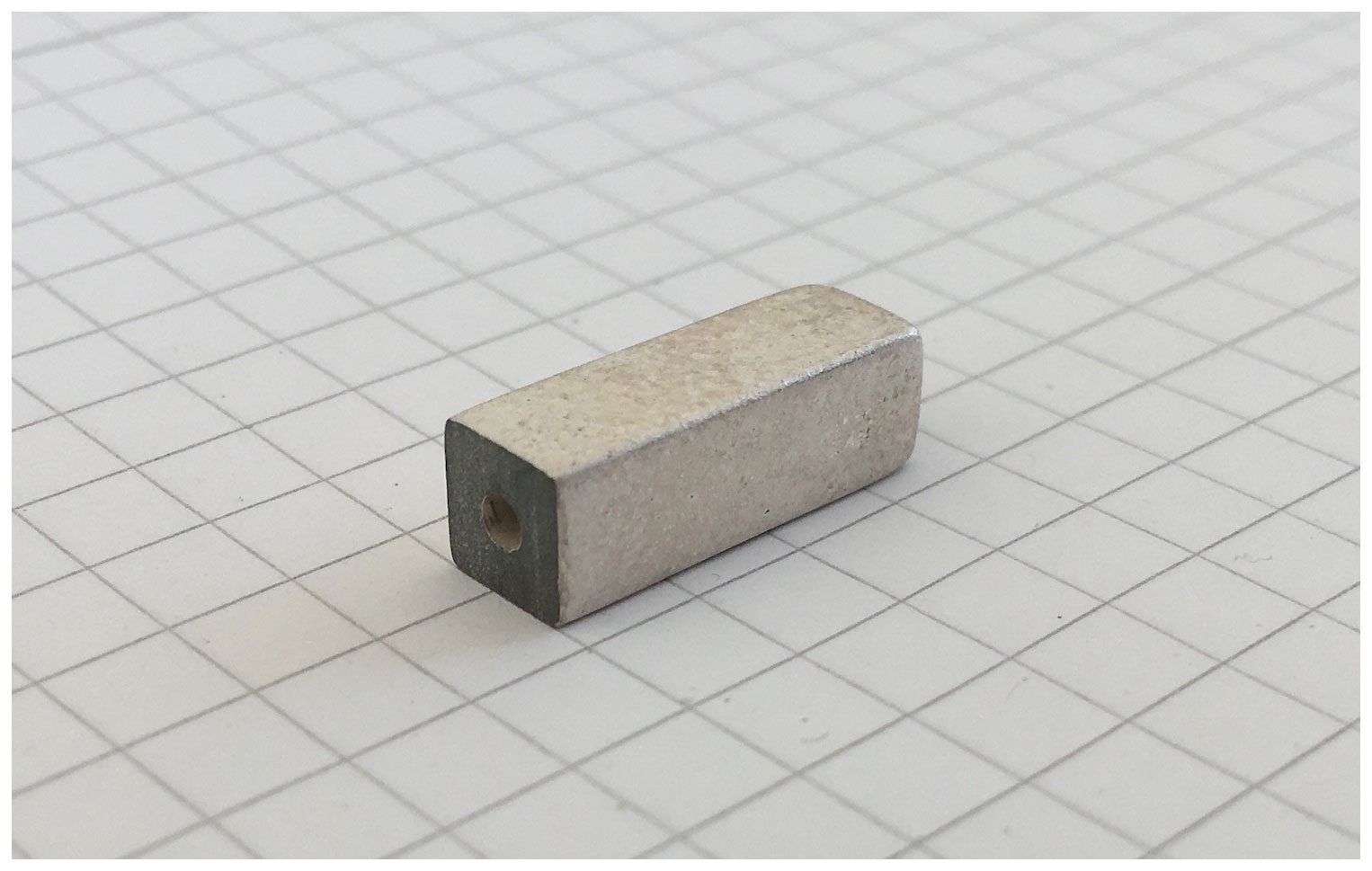
The considered ceramic resonators represent coaxial transverse electromagnetic (TEM) transmission lines with circular inner and square outer conductor, with the space in between filled by a ceramic material exhibiting a relatively large relative permittivity εr. Figure 1 shows one of the ceramic resonators used. The TLs are short-circuited by a galvanic connection between the inner and outer conductor at one end. At a specific frequency ωR, the resonator has an electrical length of and, correspondingly, a physical length l of
where λR and λ0 are the wavelengths in free space and in the dielectric, respectively. From Eq. (3), it can be seen that a larger εr would lead to a physically shorter TL length.
The characteristic impedance ZT of a TL with circular inner conductor and squared outer conductor can approximately be calculated by (Riblet, 1983)
where η0 is the free-space impedance, a1 is the side length of the squared outer conductor, a2 is the diameter of the inner conductor and γS is a factor representing the specific character of this cross section. The factor γS is considered to be γS≈1.079 (Frankel, 1942), which is expected to give good results (Cohn, 1969). With the permittivity given as εr=37 in our considerations, the characteristic impedance ZR of the ceramic resonators is calculated by Eq. (4) to be
The input impedance Zin of a short-circuited resonator without losses is
where is the propagation constant and d is the resonator length. Equating the Taylor series expansion of Eq. (6) around ω=ωR and Eq. (2) yields the element values of the equivalent PLC approximating the resonator input admittance near ωR,
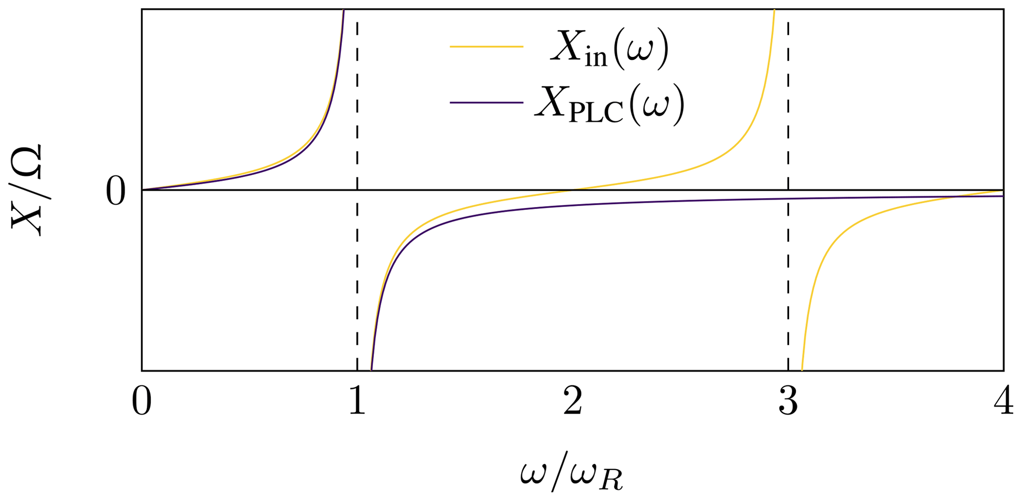
In Fig. 2, the input reactance Xin=ℑ{Zin} of a short-circuited resonator is qualitatively plotted over frequency along with the reactance XPLC=ℑ{ZPLC} of a PLC. Both resonance frequencies are ωR and XPLC approximates Xin in a certain frequency band.
The design of Chebyshev bandstop filters is straightforward, once the stopband edges ω1 and ω2, the maximum passband ripple and the degree N of the filter are known, where N will be assumed to be odd in the following such that the circuit is symmetric. The geometric mean of the band edges yields the center frequency of the stopband
and Δ is the relative bandwidth of the stopband according to
As, e.g., described in (Pozar, 2012), the element values of a lowpass prototype filter of degree N are calculated and scaled to a desired reference impedance Z0. A lowpass-to-bandstop-transformation yields a Chebyshev filter consisting of alternating SLCs and PLCs, each with the resonance frequency at ω0.
The circuit is now converted into a circuit with SLCs only by using admittance or J-inverters. These are two-ports with the property that a terminating admittance appears inverted and optionally scaled at the input port. The inverting property is frequency independent in the ideal case.
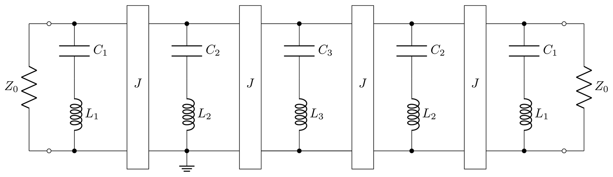
With each PLC replaced by an SLC connected to ground with one ideal admittance inverter on each side, the filter consists of SLCs and J-inverters only, see Fig. 3. The frequency response remains unchanged if the elements Li, Ci of the ith replacement SLC relate to the elements , of the ith original PLC according to
where J is measured in Ω−1.
Admittance inverters can be realized in various ways (Zverev, 2005). It can be shown that a quarter-wave TL at ω0 with characteristic impedance Z0 approximates a J-inverter in the vicinity of ω0. Other realizations are not suitable since the occurring negative element values are not feasible in our filter concept. The impact of the narrow-band approximation will be investigated together with further narrow-band restrictions in Sect. 6.
The Chebyshev filter resulting from the procedure described in Sect. 4, consisting of SLCs and quarter-wave TLs only, is the basis for the design of a bandstop filter with ceramic resonators. The method described in the following has been outlined, e.g., in (Matthaei et al., 1985).
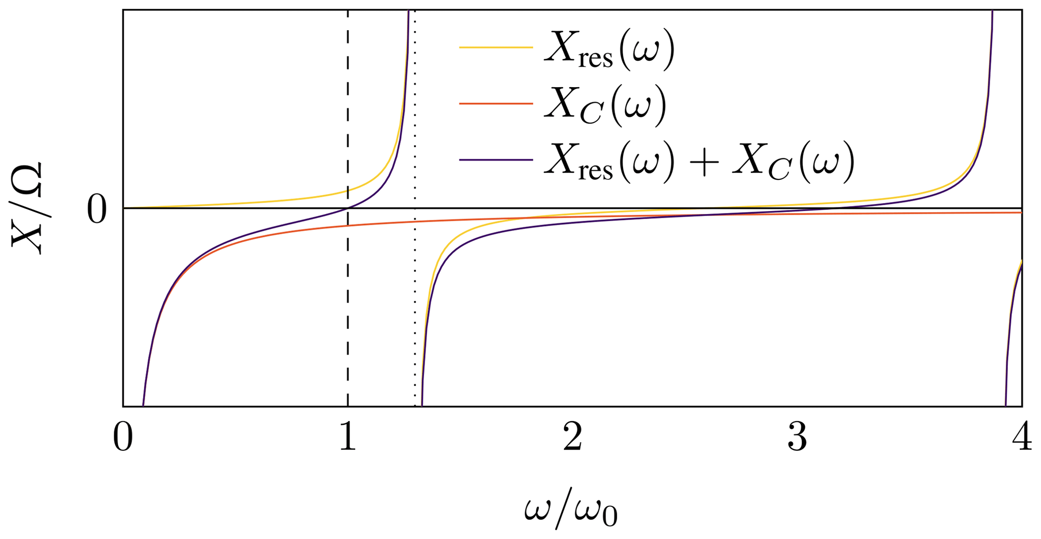
As an alternative to an SLC with the reactance vanishing at ω0, the serial connection of a capacitor and the input impedance of a resonator (SCC) as shown in Fig. 4 is considered. The electrical length ϕ of the resonator refers to ω0. If ωR>ω0, where ωR is the quarter-wave resonance frequency of the resonator, or, synonymously, , its input reactance Xres will be positive but not divergent at ω0. The negative reactance XC of a suitable capacitor added in series compensates for Xres, such that the overall impedance vanishes at ω0, just like the original SLC. This formation of the reactance root at ω0 of a SCC is shown in Fig. 5.

The proposed method maps the ith SLC to the SCC approximating the SLC near ω0 as best as possible, determining the required electrical length ϕi of the ith resonator together with an appropriate series capacitor CB,i. Replacing each SLC in Fig. 3 by the corresponding SCC and using quarter-wave TLs as J-inverters, the transformed filter response approximates the basic filter. The resulting filter circuit is shown in Fig. 6.
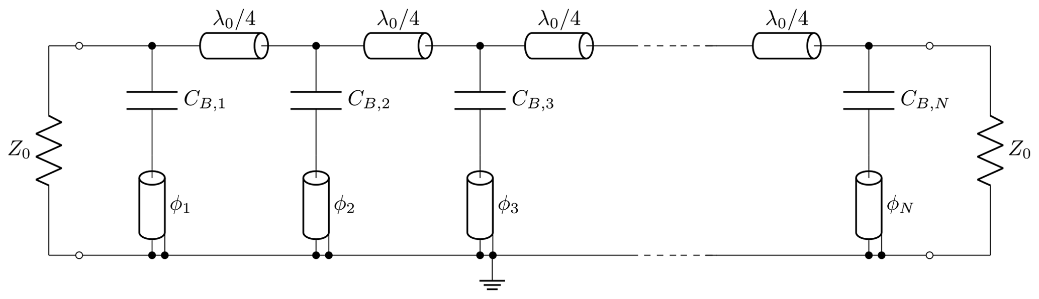
The mapping is carried out by equating the reactance slope parameters of the respective series resonant circuits, defined as (Matthaei et al., 1985)
where is the reactance of the ith SLC or SCC branch. Bringing the equation into the form of the nonlinear root-finding problem
and using the Newton-Raphson algorithm yields the required electrical length ϕi of th ith replacement SCC.
It can be shown that a solution for ϕi with always exists and that it is unique if the specifications are reasonable, i.e., non-zero and non-divergent. Because ψ is convex for , convergence of the algorithm is guaranteed if a starting value with is chosen, where is the exact solution.
Setting the SCC impedance to zero at ω0 yields
from which CB,i is calculated using the obtained ϕi.
Additional solutions for ϕi with can also exist mathematically for corresponding filter specifications. Such solutions, if existent, may lead to non-physical results or undesired filter behavior. They will not be considered further.
The SCC and SLC reactances for exemplary small and large relative bandwidths Δ are shown in Fig. 7a and b, respectively, where XSLC(ω0)=0 and XSCC(ω0)=0 are observed. The dashed line is ω=ω0, the dotted line is . Large slope parameter values correspond to a fast change of the reactance over frequency near ω0 since it is the derivative of the reactance with respect to the frequency, evaluated at ω0. Consequently, a fast change in the filter input reflection coefficient over frequency corresponds to a small Δ and vice versa.
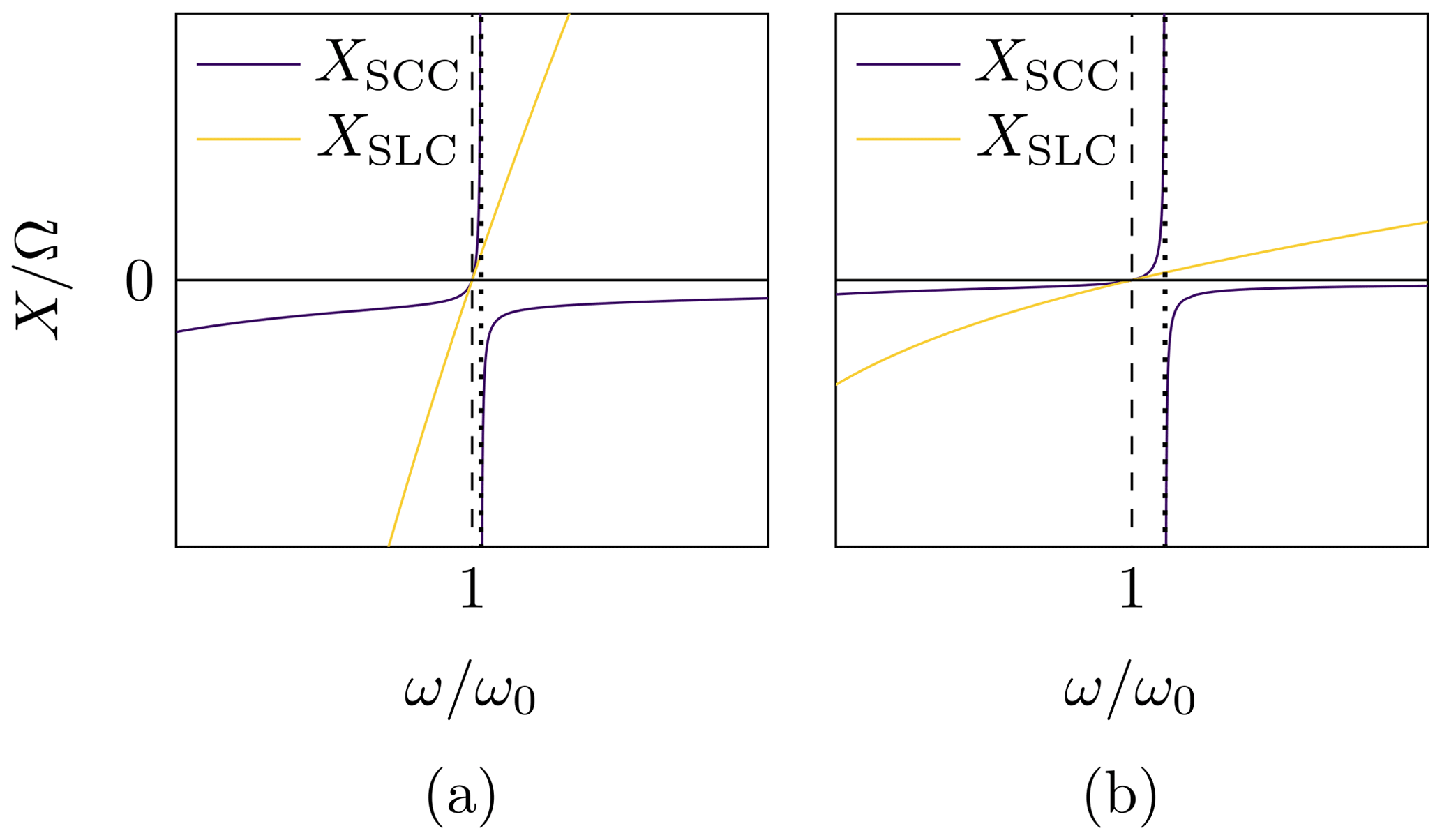
Figure 7Comparison of the reactance of an SCC with that of an SLC over frequency, for different relative bandwidths of the stopband. (a): Narrow bandwidth. (b): Large bandwidth.
In the vicinity of ω0, XSCC is convex, yielding a greater steepness slightly above ω0 than below which can also be seen from Fig. 7. Consequently, the upper stopband edge of a filter is expected to be steeper than the lower one.
The reactance approximation of an SLC by an SCC is valid only close to ω0 and quickly loses its validity when considering frequencies farther away from ω0, see Fig. 7. This effect increases with increasing relative bandwidth Δ such that additionally the approximation itself gets worse quickly. This results in a restriction of the method to narrow stopbands, additionally to the narrow-band restriction because of using quarter-wave TLs as J-inverters as described in Sect. 4.
Furthermore, denoting the individual quarter-wave resonance frequency of the ith resonator by ωR,i, the respective short-circuit termination is identically transformed into a short-circuit at 2nωR,i, n∈ℕ, and into an approximation to it at frequencies . This can be approximated by a separate SLC with its center frequency at approximately 2nωR,i at the ith branch, with the capacitor CB,i in series. Consequently, an additional bandstop effect will degrade the desired upper passband to a certain extent. The additional bandstop effect is the weaker, the smaller CB,i is. As will turn out in Sect. 8, small values of CB,i correspond to small relative bandwidths.
With all restrictions together, Δ should be limited to small values even more. Increasing N accordingly leads to even worse approximations, such that there might be a maximum N where further increase is not recommended.
Three prototypes with N=5 were designed as described in Sect. 5 for different stopband center frequencies and absolute bandwidth of GHz for each filter, resulting in a different Δ, each. The structure in which the prototypes from Sect. 8 were to be built was approximately transferred to the full-wave simulation software “CST Microwave Studio” (CST) (Dassault Systèmes, 2020), see Fig. 8.
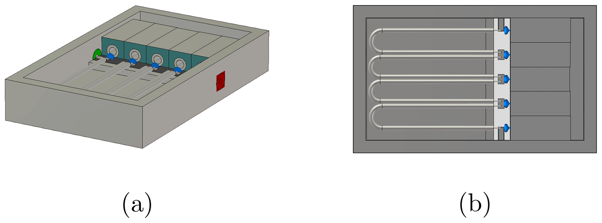
Figure 8Simulation model in CST with resonator dielectrics (dark green) and the capacitors as lumped components (blue). (a) Perspective view. (b) Top view.
The quarter-wave TLs representing the J-inverters were implemented by U-like shaped coaxial cables. This is an approximation to the actual shape, since the TLs of the hardware prototypes from Sect. 8 are wound into helices for space reasons. This structure would be very complicated to transfer to CST, apart from the fact that this would disproportionately increase the simulation time. Simulations with the U-shaped inverter lines bent upwards into closer proximity to the remaining structure showed no significant change of the filter behavior which is why this approximation of the shape is assumed appropriate.
The capacitors are each represented by lumped components in CST. One terminal of each capacitor is connected to the respective pad on a printed circuit board (PCB), onto which also the inner conductors of the neighboring semi-rigid cables are mounted. The other terminal of each capacitor is connected to the circular belt around the inner conductor of the respective resonator, which is discussed in Sect. 8.
Every metallic part is modeled as perfectly electrically conducting (PEC) and dielectric constants are purely real, no losses are considered. Parasitic effects such as electromagnetic coupling between components are expected to deteriorate the filter response to some extent.
7.1 Prototype 1
The scattering parameters |S11| and |S21| resulting from the simulation of the prototype with GHz and Δ≈2.5 % are shown over frequency in Figs. 9a, b. The desired Chebyshev frequency response in the vicinity of ω0 is identifiable but deteriorated while the stopband is shifted towards a lower center frequency , see Fig. 9a. Slightly below , |S21| collapses down to dB in a certain frequency range, see Fig. 9b, corresponding to the half-wave resonance of the individual resonators described in Sect. 6. With increasing ω, |S21| recovers first to approximately zero and collapses again notch-like slightly above . The filter can be reasonably used up to about , because the signal is attenuated too much at higher frequencies.
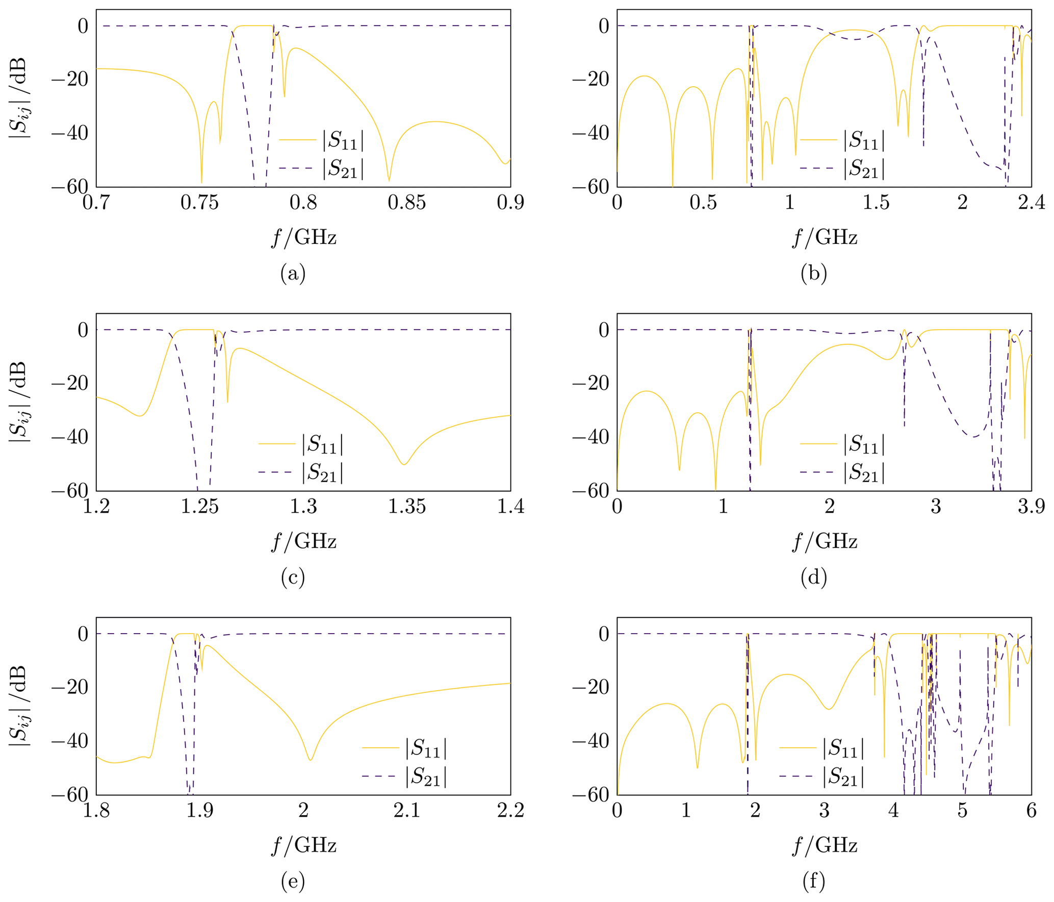
Figure 9Scattering parameters resulting from the full-wave simulation, near the respective stopbands and up to about 3ω0. (a, b): Prototype with GHz. (c, d): Prototype with GHz. (e, f): Prototype with GHz.
7.2 Prototype 2
The scattering parameters |S11| and |S21| resulting from the simulation of the prototype with GHz and Δ≈1.5 % are shown over frequency in Figs. 9c, d. The desired Chebyshev frequency response in the vicinity of ω0 is more deteriorated than for the first prototype, while the stopband is shifted towards a lower center frequency GHz, see Fig. 9c. Below , |S21| drops to a minimum of dB, recovers to approximately zero and collapses again notch-like slightly above , see Fig. 9d. It is notable that the passband drop is to a lesser extent than for the first prototype due to the lower relative bandwidth resulting from smaller CB,i values, see Sect. 6. However, the filter may also only be used reasonably up to about .
7.3 Prototype 3
The scattering parameters |S11| and |S21| resulting from the simulation of the prototype with GHz and Δ≈1 % are shown over frequency in Fig. 9e, f. The desired Chebyshev frequency response in the vicinity of ω0 is even more deteriorated than for the first two prototypes, while the stopband is shifted towards a lower center frequency GHz, see Fig. 9e. Slightly below , |S21| shows a slow break-in followed by a notch down to a minimum of dB, see Fig. 9f. The upper passband is altogether approximately zero and constant up to about , which is a significantly better performance for the upper passband than found for the first two prototypes.
The simulation results do not show an ideal Chebyshev response. At each prototype the stopband is shifted towards lower frequencies. Simulations considering losses in non-ideal materials showed no significant change in this respect. It is assumed that the discrepancies are due to the already existing complexity of the model and the associated challenges to the computational software.
The three prototypes from Sect. 7 were manufactured in hardware. Five resonators were individually cut to the respective required physical lengths from their initial length of 18 mm, with the precision of the caliper of 0.01 mm. Exploiting production tolerances, available stock capacitors were measured individually in order to meet the required capacitor values as accurately as possible.
Semi-rigid coaxial cables were cut to length with the precision again limited by the caliper and stripped afterwards at the ends, such that the section of the cable with outer conductor corresponds to an electric length of . The resulting TL sections are used as J-inverters. The inner conductor stands out a little to solder it to the respective pad as can be seen in Fig. 8.
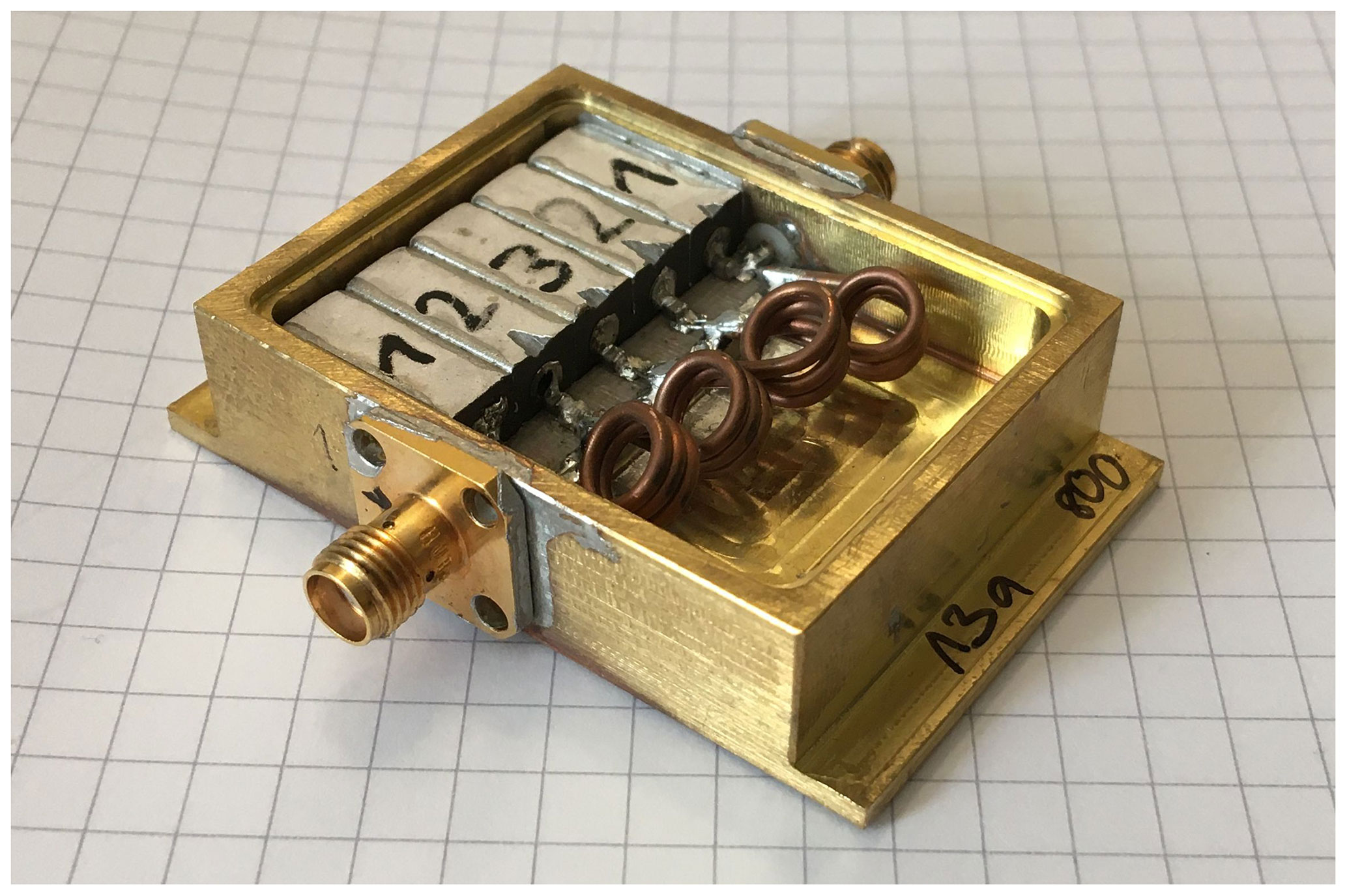
To provide a fixture for the capacitors and the coaxial cables, a PCB was designed with N pads on it in front of the resonators. The outer two resonators were connected to the respective inner conductors of the coaxial terminals via the series capacitors CB,1 and CB,N. Since the inner conductor of the resonators only consists of the coating of the ceramic material inside the resonator, where the capacitors can not be soldered onto, conducting ferrules were inserted into the resonators, building a flattened circular belt around the cannulation. One of the capacitor terminals is soldered to the belt, the other one is connected to the inner conductors of the neighboring semi-rigid cables. A photograph of one of the prototypes is shown in Fig. 10, where the small cuts at the upper resonator edges result from the tuning process. The other two prototypes are identical in construction except for different element values resulting from the design.
After assembling the whole filter, the frequency response was first measured directly without any adjustment, see Fig. 11 for the neighborhood of the respective center frequencies. By a subsequent, targeted manipulation of the circuit, the prototypes were improved in terms of a best possible Chebyshev-like frequency response to meet the specifications in center frequency and bandwidth as well as possible. This filter tuning process is discussed in the following.
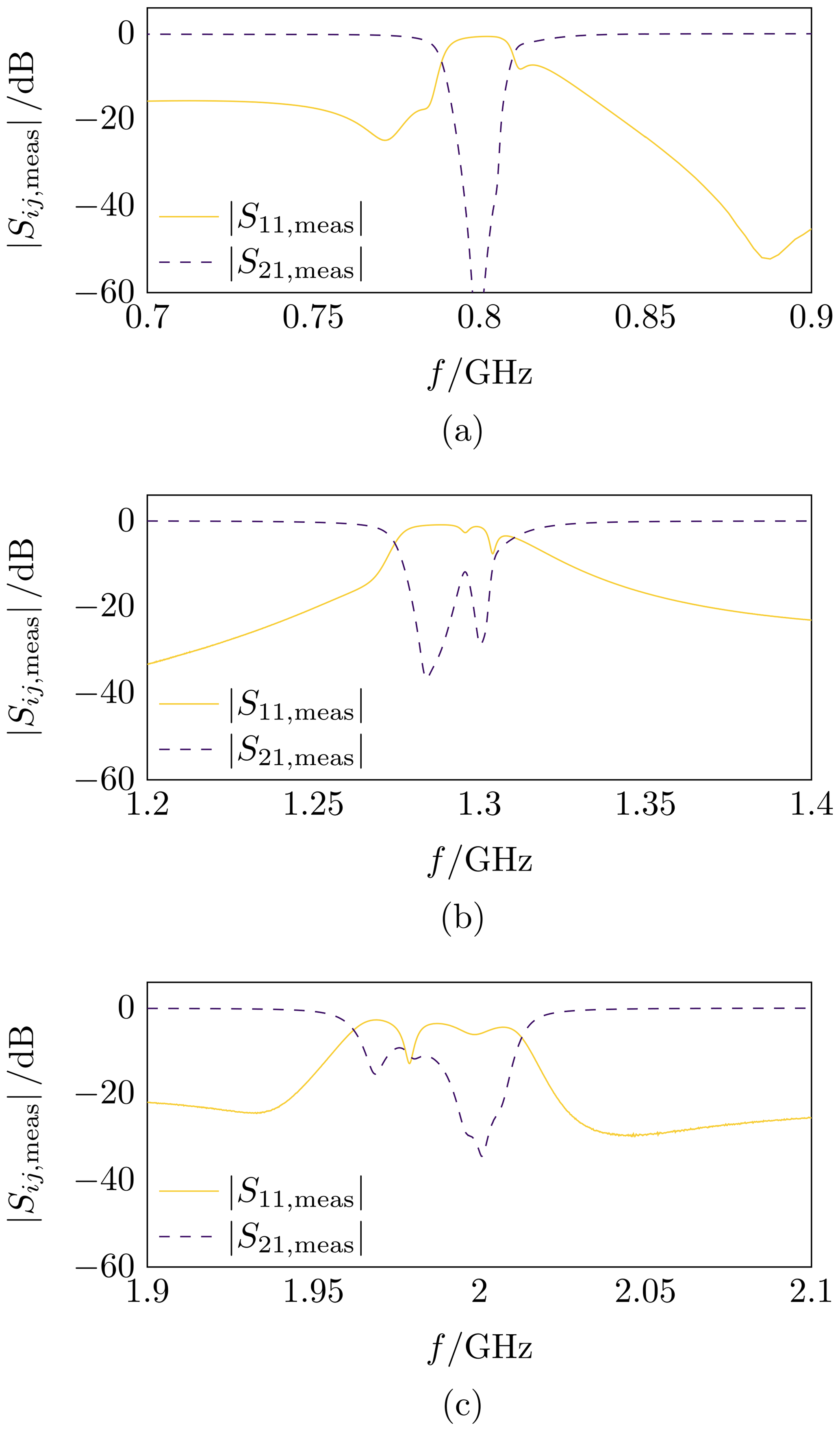
Figure 11Measured scattering parameters before tuning, in the vicinity of the respective stopbands. (a): Prototype with GHz. (b): Prototype with GHz. (c): Prototype with GHz.
For an ideal Chebyshev filter, each branch is resonant at ω0. The ith branch of a manufactured filter in general resonates at effectively, which is because of manufacturing tolerances and parasitic effects in the filter structure. By adjusting the element values ϕi and the capacitor CB,i of the N branches, the filter response should be transformed into a Chebyshev-like frequency response satisfying given specifications as close as possible.
All manipulations are carried out in situ to avoid thermal stress by disassembling the filter once for each tuning step. However, occurring parasitics are not completely predictable and would generally change after each reassembly, especially at higher frequencies, which is also why disassembling the whole filter is not recommended.
In the following, the impact of ϕi and CB,i manipulations on the frequency response of one individual branch is considered. Since the filter consists of N branches, it is assumed that the impact on one filter branch qualitatively influences the frequency response of the whole filter. Practice shows that this assumption is appropriate.
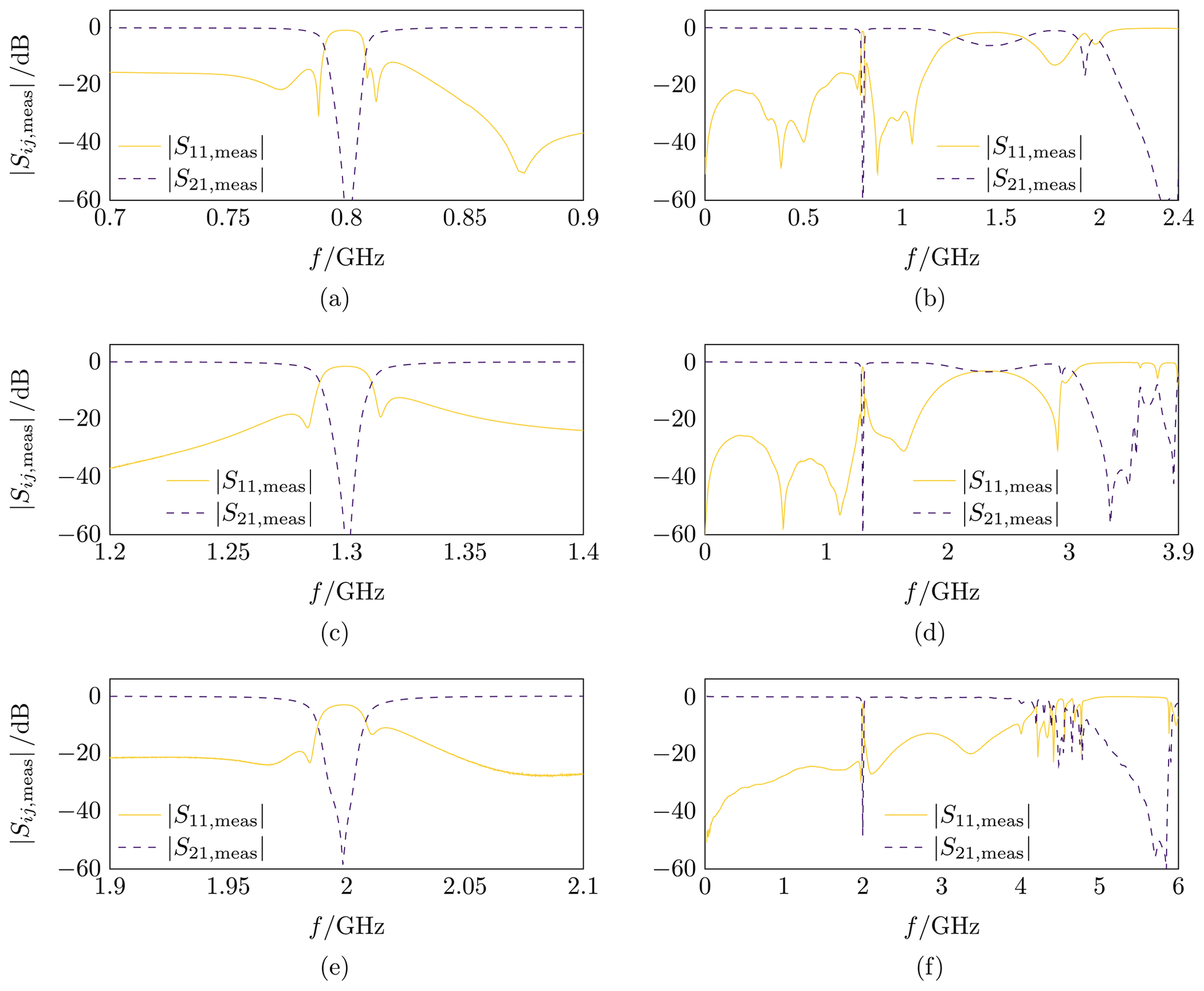
Figure 12Measured scattering parameters resulting after tuning, near the respective stopbands and up to about 3ω0. (a, b): Prototype with GHz. (c, d): Prototype with GHz. (e, f): Prototype with GHz.
The impact of a change in ϕi on ω0,i is investigated by rearranging Eq. (13) and taking the derivative with respect to ϕi, yielding
Enlarging the ith resonator will, therefore, decrease, shortening it will increase the resonance frequency ω0,i of the corresponding branch, respectively. Analogously, the impact of a change in CB,i on ω0,i is investigated by rearranging Eq. (13) and taking the derivative with respect to CB,i,
Enlarging the ith capacitor will, therefore, decrease, reducing it will increase the resonance frequency of the corresponding branch, respectively.
To investigate the impact of changes in ϕi or CB,i on the bandwidth of the ith branch, the slope parameter serving as measure for bandwidth could be consulted by taking the derivative of xSCC,i with respect to either of ϕi or CB,i. However, it should be noted that by changing these parameters independently, ω0,i is also changed as was shown before. Since the slope parameter is defined by evaluating the derivative of the branch reactance at ω0,i, it will not be exact anymore. Considerations analogue to the preceding ones can, therefore, not be made without introducing an approximation, which gets worse with larger modifications.
With knowledge of the aforementioned, taking the derivative of xSCC,i with respect to ϕi qualitatively yields
implying that an increasing ϕi will lead to an increasing xSCC,i and, thus, to a narrower bandwidth of the stopband and vice versa, as described in Sect. 5. Analogously, taking the derivative of xSCC,i with respect to CB,i qualitatively yields
implying that an increasing CB,i will lead to a decreasing xSCC,i and, thus, to a larger bandwidth of the stopband and vice versa. Frequency shifts occurring while tuning the bandwidth are compensated for by using Eq. (14), which in turn will have an influence on the bandwidth. The tuning may, therefore, need a number of iterations until the specifications are met.
An effective shortening of the built-in resonator length ϕi can be achieved by cutting into the ith resonator at the upper edge as observable in Fig. 10. The frequency increasing effect of this cutting can be shown by simulation of a single resonator with a cut at the same place and observing its quarter-wave resonance frequency with increasing cut depth. This only works with a limited cutting depth as the resonator obviously gets defaced otherwise.
Electrically increasing the length can be done by adding a piece of metal or solder to the ferrule. This acts as an additional capacitance between inner conductor and ground, added in parallel to the equivalent PLC approximating the TL. From Eq. (1), it can be seen that the resonance frequency thereby decreases.
Increasing the capacitor values is carried out by exchanging it to another one or, if the effect should be rather small, mounting a piece of metal to one of its terminals. Doing so, a capacitor with air as dielectric is effectively added in parallel. It is advisable to perform this at the side facing away from the resonator to avoid possible influence on the resonator. A smaller capacitance can be achieved by replacing it by one with a smaller value or by removing solder around the capacitor, if present.
The influence of individual tuning steps can be observed using a vector network analyzer. After few iterations, the filters were significantly improved in performance. To preserve the symmetry of odd-N Chebyshev filters, both and should be achieved.
The resulting frequency responses of the tuned filter prototypes are shown in Fig. 12. The individual bandwidths can not exactly be adjusted to meet the specification because the |S21| ripples do not exist. This fact is assumed to be a consequence of parasitics, losses and radiation from the structure. Nevertheless, the shape of |S11| in the stopband, corresponding to supposed |S21| ripples, is recognizable, in particular see Fig. 12a. Towards higher center frequencies, the oscillation in |S11| is qualitatively reduced, see Fig. 12c and e. This effect is assumed to be due to stronger parasitics at higher frequencies. Considering frequencies beyond the corresponding stopbands, see Fig. 12b, d and f, again the transmission drop in the upper passband, as described in Sect. 6, is observed. Its impact decreases with decreasing Δ.
The filter design method investigated in this paper was able to reasonably approximate Chebyshev bandstop filters by solving a series of one-dimensional, non-linear root finding problems, carried out by Newton's method and with guaranteed convergence.
The manufactured filters were slightly shifted away from the desired center frequency, which could be corrected for by applying the described tuning methods. Approximate Chebyshev behavior at the respective desired stopband frequencies was observable together with reasonable passband performance below the stopband and above, the latter under the premise that the relative stopband bandwidth is small enough.
Filters with order 5 and a relative bandwidth of <1 % seem to show good performance in the upper passband. In order to generalize this approach to larger filter orders, further prototypes have to be built, tuned and characterized. It is expected that the approximation to a Chebyshev filter qualitatively degrades with increasing filter order since the assumed approximations become worse.
The underlying research codes can be requested from the authors.
The underlying research data can be requested from the authors.
JFT worked out the underlying theory, built the filter prototypes and carried out simulations and measurements. TFE helped with the theory part and supervised the documentation. All authors read and approved the final manuscript.
The authors declare that they have no conflict of interest.
Publisher’s note: Copernicus Publications remains neutral with regard to jurisdictional claims in published maps and institutional affiliations.
This article is part of the special issue “Kleinheubacher Berichte 2020”.
This work has been carried out at Wainwright Instruments GmbH, http://www.wainwright-filters.com (last access: 15 July 2021), DE-82346 Andechs. The authors are grateful to Wainwright Instruments for this support.
This paper was edited by Romanus Dyczij-Edlinger and reviewed by two anonymous referees.
Cohn, S. B.: Beating a problem to death, Microwave J., 12, 22–24, 1969. a
Dassault Systèmes: CST Microwave Studio 2020, available at: https://www.3ds.com/products-services/simulia/products/cst-studio-suite/ (last access: 12 July 2021), 2020. a
Frankel, S.: Characteristic impedance of parallel wires in rectangular troughs, Proceedings of the IRE, 30, 182–190, https://doi.org/10.1109/JRPROC.1942.234653, 1942. a
Gurov, E. V., Uvaysov, S. U., Uvaysova, A. S., and Ivanov, I. A.: Analysis of the parasitic parameters influence on the analog filters frequency response, in: International Seminar on Electron Devices Design and Production (SED), Prague, Czech Republic, https://doi.org/10.1109/SED.2019.8798382, pp. 1–7, 2019. a
Martin, F., Falcone, F., Bonache, J., Marques, R., and Sorolla, M.: Miniaturized coplanar waveguide stop band filters based on multiple tuned split ring resonators, IEEE Microw. Wirel. Co., 13, 511–513, https://doi.org/10.1109/LMWC.2003.819964, 2003. a
Matthaei, G. L., Young, L., and Jones, E. M. T.: Microwave Filters, Impedance-Matching Networks, and Coupling Structures, Artech House, Norwood, MA, reprint of the ed. publ. by macgraw-hill 1964 edn., 1980. a, b
Pozar, D. M.: Microwave Engineering, 4th edn., John Wiley & Sons Inc., Hoboken, NJ, 2012. a, b
Riblet, H.: An accurate approximation of the impedance of a circular cylinder concentric with an external square tube, IEEE T. Microw. Theory, 31, 841–844, https://doi.org/10.1109/TMTT.1983.1131615, 1983. a
Schiffman, B.: Correction to “Exact design of band-stop microwave filters”, IEEE T. Microw. Theory, 13, 703, https://doi.org/10.1109/TMTT.1965.1126090, 1965. a
Schiffman, B. and Matthaei, G.: Exact design of band-stop microwave filters, IEEE T. Microw. Theory, 12, 6–15, https://doi.org/10.1109/TMTT.1964.1125744, 1964. a
Sorkherizi, M. S. and Kishk, A. A.: Bandstop filters on double ridge waveguide with wide matched passbands, in: 17th International Symposium on Antenna Technology and Applied Electromagnetics (ANTEM), Montreal, QC, Canada, 10–13 July 2016, https://doi.org/10.1109/ANTEM.2016.7550130, pp. 1–2, 2016. a
Zverev, A. I.: Handbook of Filter Synthesis, Wiley-Interscience, Hoboken, NJ, 2005. a
- Abstract
- Introduction
- Lumped resonant circuits
- Ceramic Resonators
- Design of Lumped Element Chebyshev Filters
- Approximate Design by Slope Parameters
- Restrictions to narrow stopbands
- Full-wave simulation
- Fabricated filter prototypes and tuning
- Conclusions
- Code availability
- Data availability
- Author contributions
- Competing interests
- Disclaimer
- Special issue statement
- Acknowledgements
- Review statement
- References