Articles | Volume 19
https://doi.org/10.5194/ars-19-79-2021
17 Dec 2021
 | 17 Dec 2021

A Low-Power Squaring Circuit with Regulated Output and Improved Settling Time in 180 nm CMOS for 3–5 GHz IR-UWB Applications

Daniel Schrüfer, Jürgen Röber, Timo Mai, and Robert Weigel
Abstract

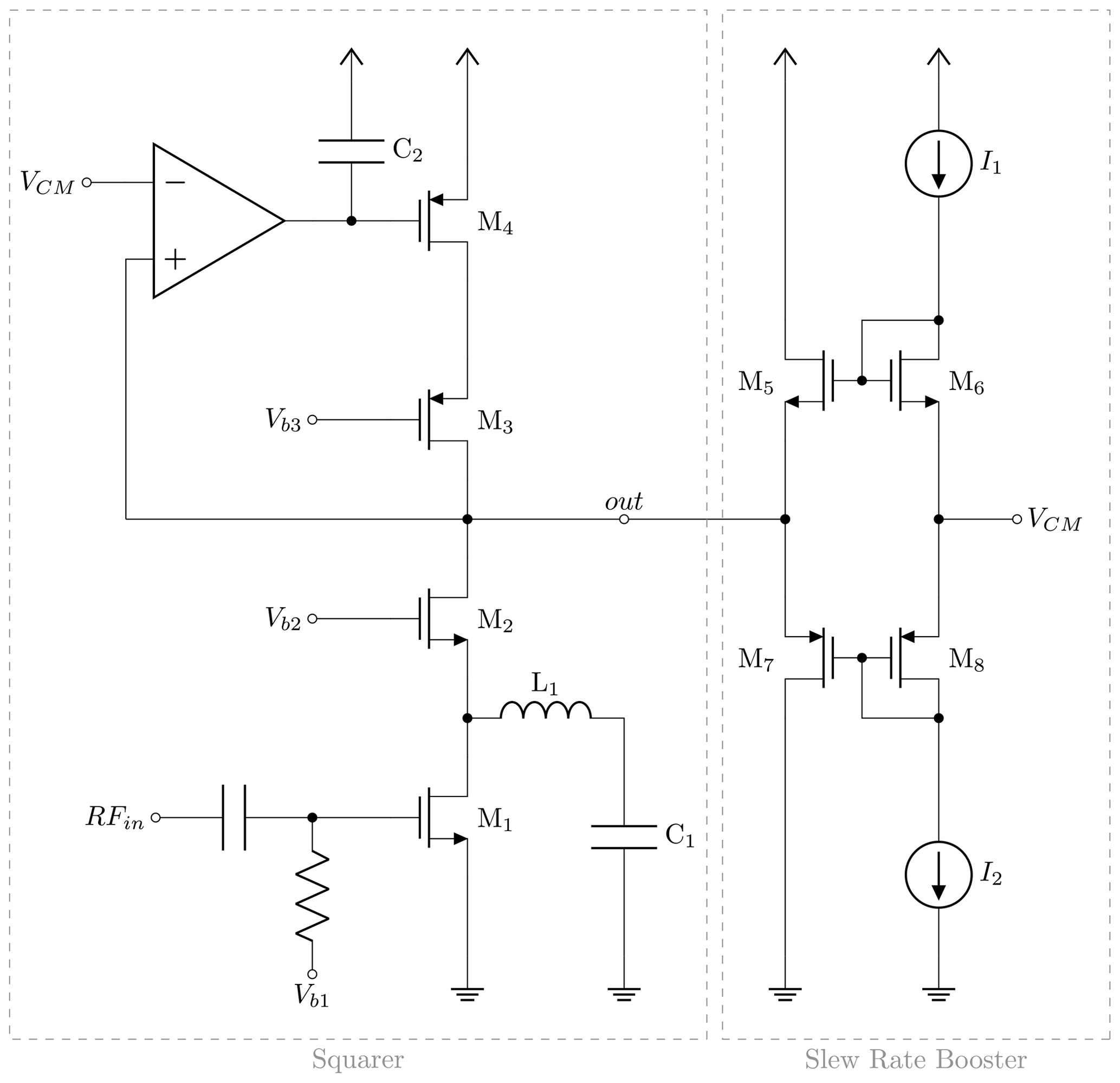
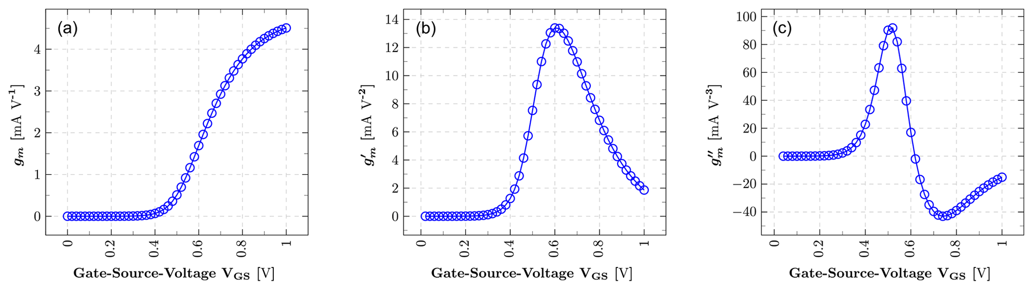
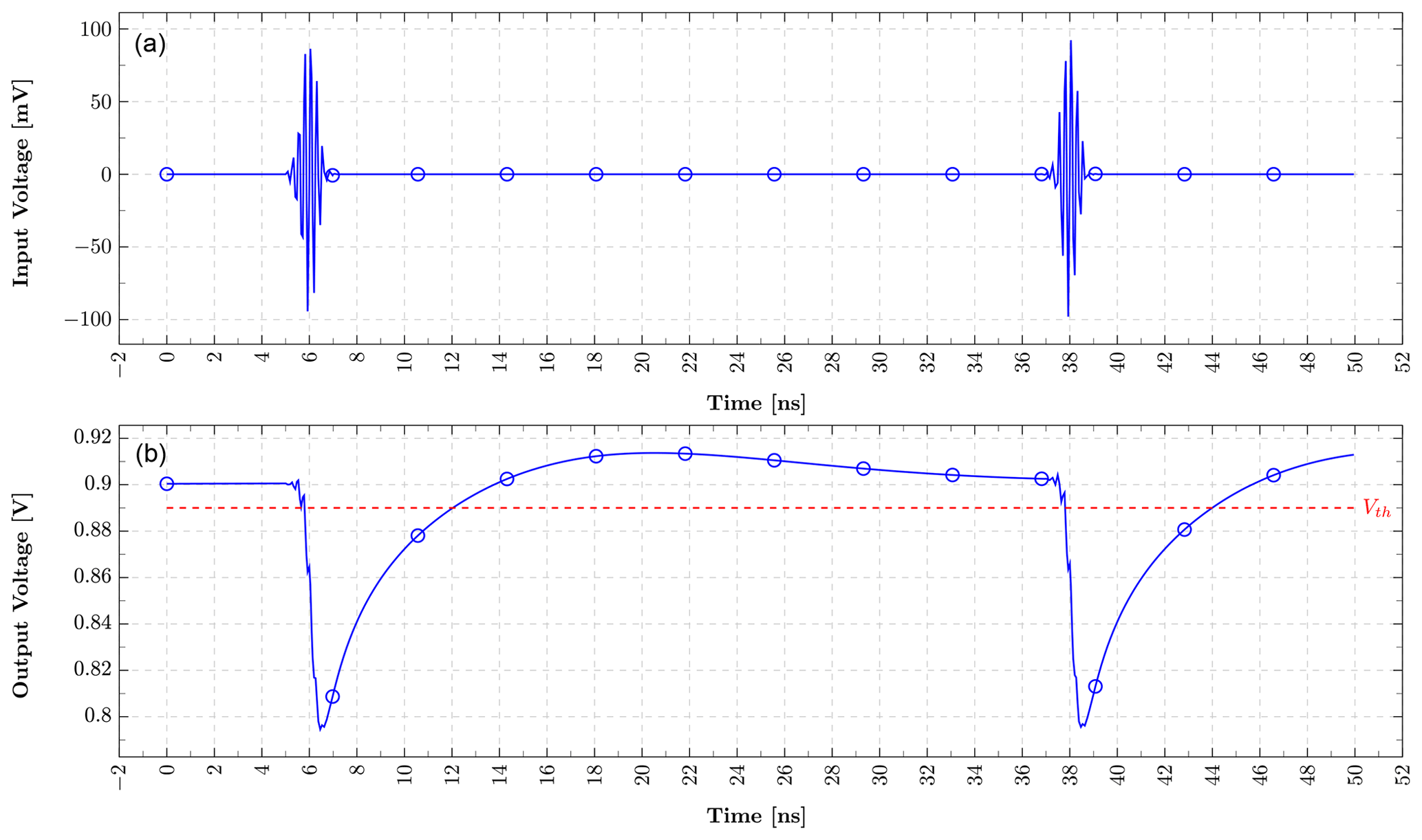
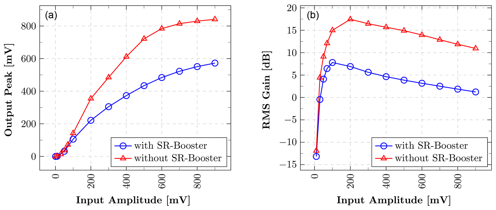
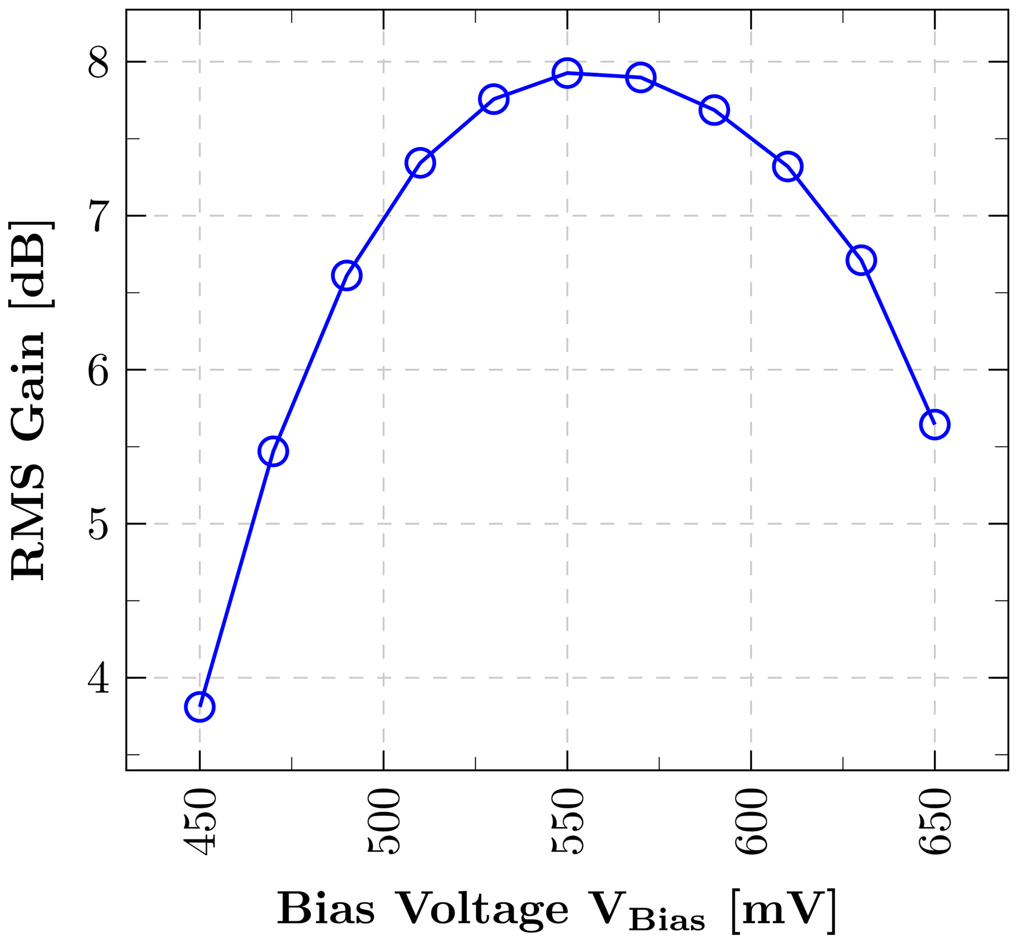
This paper demonstrates a low-power squaring circuit for 3–5 GHz non-coherent Impulse-Radio Ultra-Wideband (IR-UWB) receivers for Pulse Position Modulation (PPM) in a low-cost 180 nm CMOS technology. The squaring, which is the key element in typical IR-UWB receivers, is performed exploiting the non-linear transfer function of a MOS transistor. For a high gain at low power consumption the transistor is biased in the moderate inversion region, where the second-order derivative of the transconductance gm and, as a result, the quadratic term in the transfer function reaches a maximum. A control loop was implemented to set the dc output voltage to a defined value and thus to allow a comparison of the squarer output signal with a defined threshold voltage, which can easily be set and adjusted (e.g. by a DAC). To speed up the settling time of the output and hence to reach higher data rates, a novel slew-rate booster is implemented at the output. Thereby, the squarer is capable of data rates of up to 15.6 Mbit s−1, which is more than two times higher compared to the circuit without the slew-rate booster, while only consuming 72.4 µW in addition. In the extracted post-layout simulations the whole circuitry consumes 724 µA at a 1.8 V power supply, resulting in a power consumption of 1.3 mW.

Dates
1 Introduction

With the evolution of Internet of Things (IoT) and the emergence of Body Area Networks, the demand for low-power transceiver systems has increased. A promising candidate for this kind of communication is Impulse-Radio Ultra-Wideband (IR-UWB) technology, which is capable of low-power high-speed communication over short distances using simple modulation schemes like On-Off-Keying (OOK) or Pulse Position Modulation (PPM) (Thotahewa et al.2014; Daoud et al.2014; Crepaldi et al.2011).

A typical way to receive this kind of signals is by squaring and integrating them. This can be done in various ways ranging from multiplying the signal with itself using active (Stoica et al.2006; Xia et al.2011) or passive mixers (Tuan-Anh Phan et al.2007) or by squaring the signal exploiting the transfer characteristic of a MOS transistor (Parvizi et al.2012).

This paper proposes a low-power squaring circuit for 3–5 GHz IR-UWB applications for PPM, which also exploits the MOS transistor's transfer characteristics for the squaring. For the sake of higher speed and hence higher data rates, it also consists of a slew rate booster.

The paper is organized in four sections: Sect. 2 illustrates the concept and circuit architecture, Sect. 3 summarizes the simulation results, and Sect. 4 concludes the paper.

https://ars.copernicus.org/articles/19/79/2021/ars-19-79-2021-f01

Figure 1Schematic of the complete squaring circuit.

Download

https://ars.copernicus.org/articles/19/79/2021/ars-19-79-2021-f02

Figure 2gm (a), its first-order derivate gm (b) and its second-order derivate gm′′ (c) over the gate-source-voltage VGS for a NMOS with W=10µm, L=180nm and VDS = 0.5V.

Download

2 Low-Power Squaring Circuit

The schematic of the proposed squaring circuit is shown in Fig. 1. It is built up in a single-ended structure to reduce the power consumption – not only for the squarer itself but also for the preceding amplifier. The circuit consists of a squaring part, a control loop for the dc output voltage, and a slew-rate booster. Each one of these parts is described in the following subsections.

2.1 Squarer

To detect an incoming RF signal of the form vRF(t)=Acosωt, the envelope is extracted by squaring the input signal resulting in

(1) v RF 2 ( t ) = A 2 cos 2 ω RF t = A 2 2 + A 2 2 cos 2 ω RF t ,

and filtering out the high frequency parts.

The squaring of the RF input signal is performed by the input transistor M1 exploiting the non-linear MOS transfer function. Considering the Taylor series of the small signal drain current

(2) i DS ( t ) = g m v GS ( t ) + 1 2 ! g m v GS 2 ( t ) + 1 3 ! g m ′′ v GS 3 ( t ) + ,

where gm denotes the transconductance, and gm and gm′′ are its first and second-order derivatives with respect to the gate-source voltage vGS, it reveals that the drain current contains a term of the squared input voltage and thus fulfils the desired squaring operation (Parvizi et al.2012; Byeon et al.2011).

As apparent in Eq. (2), to maximize the squaring gain, the first-order derivative of the transconductance gm has to be maximized. This is accomplished by biasing the transistor in the moderate inversion region between sub-threshold and strong inversion region, where the current flow mechanism changes from diffusion to drift causing a maximum of gm (see Fig. 2) (Parvizi et al.2012; Toole et al.2004).

To extract the desired term of the output in Eq. (2), the unwanted fundamental wave gmvGS(t) is suppressed by the LC Filter of L1 and C1 (Byeon et al.2011), which has a better filter performance in the desired frequency band compared to a simple capacity but at the cost of an extra chip area of 175 µm× 175 µm. The higher order term 13!gm′′vGS3(t) on the other hand is nearly zero due to the biasing in the moderate inversion region. In this region gm reaches a maximum and therefore, its derivative gm′′ passes through zero (see Fig. 2) (Toole et al.2004; Parvizi et al.2012).

https://ars.copernicus.org/articles/19/79/2021/ars-19-79-2021-f03

Figure 3Telescopic Operational Transconductance Amplifier (OTA).

Download

2.2 Control Loop

The control loop was implemented to set the dc output voltage to a defined value. In this way it is possible for a comparator to compare the squarer output signal with a defined threshold voltage. This threshold voltage can easily be set and adjusted (e.g. by a DAC) depending on factors like the needed sensitivity or the robustness against interference and noise. This adjustable threshold takes also the DC-regulation loop and the comparator offset into account. A possible comparator threshold voltage is illustrated in Fig. 6.

The control loop was realized with a telescopic OTA (Operational Transconductance Amplifier) because of its simple architecture, its high dc gain and its power efficiency (see Fig. 3). The speed of the control loop has to be slow to not attenuate the desired output signal. For this reason and for the purpose of stability, the capacity C2 was inserted at the OTA's output (see Fig. 1).

https://ars.copernicus.org/articles/19/79/2021/ars-19-79-2021-f04

Figure 4Input resistance of the slew-rate booster over the input voltage.

Download

https://ars.copernicus.org/articles/19/79/2021/ars-19-79-2021-f05

Figure 5Settling of the output peak with and without the slew-rate booster for a 200 mV input amplitude.

Download

https://ars.copernicus.org/articles/19/79/2021/ars-19-79-2021-f06

Figure 6Input (a) and output voltage (b) of the squarer for a input amplitude of 100 mV and a dc output voltage VCM=900mV. The dashed line illustrates a possible threshold voltage of a subsequent comparator.

Download

https://ars.copernicus.org/articles/19/79/2021/ars-19-79-2021-f07

Figure 7Output peak voltage (a) and RMS gain (b) over the input amplitude.

Download

2.3 Slew-Rate Booster

Due to the high output resistance, which is necessary for a high gain at low input voltages, after the appearance of a PPM pulse the output node voltage settles back to its dc voltage only with limited speed and hence limits the maximum data rate. To enhance this settling time after an incoming PPM pulse, a faster control loop is not suitable as it would attenuate the desired output peak. Thus, an output-level dependent slew-rate booster is added to the output of the squarer.

This slew-rate booster is depicted on the right side of Fig. 1. It consists of one NMOS current mirror (M5, M6), one PMOS current mirror (M7, M8), and two current sources I1 and I2, which both are biased with the same current.

The input resistance of the slew-rate booster is

(3) R in 1 g m , M 5 + g mb , M 5 | | 1 g m , M 7 + g mb , M 7

where gm,M5 and gm,M7 are the transconductances of M5 and M7 and gmb,M5 and gmb,M7 being the bulk transconductances of M5 and M7 (Razavi2000). With gm and gmb of M5 and M7 depending on the input voltage of the slew-rate booster, the circuit forms a non-linear resistance with a large value for small signals and a smaller value for larger ones (see Fig. 4). Thus, small output peaks of the squarer will not be attenuated whereas larger output peaks will be attenuated to settle faster.

The enhanced settling speed of the circuit with the slew-rate booster can be observed in Fig. 5, where the output peak of the squarer is plotted with and without the slew-rate booster for an input amplitude of 200 mV. As the output resistance is higher without the slew-rate booster, there is a bigger peak appearing at the output, which settles back slower. Due to the larger output resistance, the overall loop gain is higher and the non-dominant output pole is shifted to lower frequencies resulting in a low phase margin and an overshooting behaviour. This can be reduced by increasing the capacity C2 at the OTA's output, but, however, at the cost of an even slower settling.

3 Simulation Results

The squaring circuit is developed in a 180 nm CMOS technology. The following results are from post-layout simulations including all parasitic elements.

Figure 6 shows the typical input signal of the squarer, which is formed by a Gaussian pulse, and its corresponding output peak. For a 15.6 Mbit s−1 PPM signal the incoming 4 GHz pulse has a duration of 2 ns followed by an at least 30 ns lasting pause depending on the bit sequence. Thus, the output has to settle back to a tolerance range around its dc voltage which depends on the comparator's threshold within this 32 ns. The dc output voltage VCM was chosen to 0.9 V.

For an incoming signal with a data rate of 15.6 Mbit s−1, the squaring circuit reaches a gain as shown in Fig. 7 while drawing a dc current of 724 µA at 1.8 V power supply.

Figure 7 plots the output peak voltage of the squarer as well as the RMS gain over its input amplitude with and without the slew-rate booster enabled. Due to squaring characteristics the gain is small for low input amplitudes and rises for larger ones. For low input amplitudes both circuits, the one with and the one without the slew-rate booster, have similar gain curves, which, however, diverge for larger amplitudes, where the output peak is high enough to be detectable and the slew-rate booster is taking over resulting in a gain drop. At even higher input voltages saturation sets in further reducing the gain.

As already discussed before, the gain of the squarer depends on the magnitude of gm, which again is affected by the bias voltage of the squaring transistor. Thus, it's advisable to examine the effect of bias voltage variations on the squarer's gain. Figure 8 shows the RMS gain of the circuit over the gate-source-voltage of the input transistor. The maximum is achieved for a gate-source-voltage of around 560 mV, which is in accordance with Fig. 2. For a bias voltage variation of ± 10 % the gain is reduced by less than 1 dB.

https://ars.copernicus.org/articles/19/79/2021/ars-19-79-2021-f08

Figure 8RMS gain over the biasing voltage of the input transistor for an input amplitude of 100 mV.

Download

4 Conclusions

This paper demonstrated a low-power squaring circuit with a controlled dc output voltage for impulse-radio ultra-wideband applications operating in the frequency range of 3–5 GHz. Due to a fast, novel slew-rate booster, which only consists of two current sources and two current mirrors, the settling time at the output has been decreased, whereby the circuit is capable of processing data rates of 15.6 Mbit s−1 for pulse-position modulated signals. This data rate is more than two times higher compared to the circuit without the slew-rate booster, while only consuming 72.4 µW in addition. The dc current consumption of the whole squaring circuit is 724 µA at a 1.8 V power supply resulting in a power consumption of 1.3 mW.

Data availability

The data presented in this article are available from the author upon request.

Author contributions

DS developed the circuit and did the simulations. JR and TM supported with ideas, feedback and fruitful discussions. RW's contribution included mentorship and feedback. He supervised the project and provided resources.

Competing interests

The authors declare that they have no conflict of interest.

Disclaimer

Publisher's note: Copernicus Publications remains neutral with regard to jurisdictional claims in published maps and institutional affiliations.

Special issue statement

This article is part of the special issue “Kleinheubacher Berichte 2020”.

Financial support

This research has been supported by the German Federal Ministry of Education and Research (BMBF) through the project MR-Implant (grant no. 16ES0766).

Review statement

This paper was edited by Jens Anders and reviewed by Hadi Lotfi and one anonymous referee.

References

Byeon, C. W., Lee, J. J., Eun, K. C., and Park, C. S.: A 60 GHz 5 Gb/s Gain-Boosting OOK Demodulator in 0.13 µm CMOS, IEEE Microw. Wirel. Co., 21, 101–103, https://doi.org/10.1109/lmwc.2010.2096411, 2011. a, b

Crepaldi, M., Li, C., Fernandes, J. R., and Kinget, P. R.: An Ultra-Wideband Impulse-Radio Transceiver Chipset Using Synchronized-OOK Modulation, IEEE J. Solid-St. Circ., 46, 2284–2299, https://doi.org/10.1109/JSSC.2011.2161214, 2011. a

Daoud, M., Ghorbel, M., and Mnif, H.: A non-coherent high speed IR-UWB receiver for biomedical implants, in: 2014 1st International Conference on Advanced Technologies for Signal and Image Processing (ATSIP), IEEE, Sousse, Tunisia, 533–538, https://doi.org/10.1109/ATSIP.2014.6834672, 2014. a

Parvizi, M., Allidina, K., and El-Gamal, M. N.: An ultra low power, low voltage CMOS squarer circuit for non-coherent IR-UWB receivers, in: 2012 IEEE International Symposium on Circuits and Systems, IEEE, Seoul, South Korea, 2533–2536, https://doi.org/10.1109/ISCAS.2012.6271819, 2012. a, b, c, d

Razavi, B.: Design of Analog CMOS Integrated Circuits, McGraw-Hill, New York, NY, USA, 2000. a

Stoica, L., Rabbachin, A., and Oppermann, I.: A low-complexity noncoherent IR-UWB transceiver architecture with TOA estimation, IEEE T. Microw. Theory, 54, 1637–1646, https://doi.org/10.1109/TMTT.2006.872056, 2006. a

Thotahewa, K. M. S., Redoute, J., and Yuce, M. R.: Hardware implementation of an IR-UWB coordinator node for WBAN applications, in: 2014 IEEE 25th Annual International Symposium on Personal, Indoor, and Mobile Radio Communication (PIMRC), IEEE, Washington, DC, USA, 2168–2172, https://doi.org/10.1109/PIMRC.2014.7136532, 2014.  a

Toole, B., Plett, C., and Cloutier, M.: RF circuit implications of moderate inversion enhanced linear region in MOSFETs, IEEE T. Circuits I, 51, 319–328, https://doi.org/10.1109/TCSI.2003.822400, 2004. a, b

Tuan-Anh Phan, Krizhanovskii, V., and Sang-Gug Lee: Low-Power CMOS Energy Detection Transceiver for UWB Impulse Radio System, in: 2007 IEEE Custom Integrated Circuits Conference, IEEE, San Jose, CA, USA, 675–678, https://doi.org/10.1109/CICC.2007.4405822, 2007. a

Xia, L., Shao, K., Chen, H., Huang, Y., Hong, Z., and Chiang, P. Y.: 0.15-nJ/b 3–5-GHz IR-UWB System With Spectrum Tunable Transmitter and Merged-Correlator Noncoherent Receiver, IEEE T. Microw. Theory, 59, 1147–1156, https://doi.org/10.1109/TMTT.2011.2114193, 2011. a

Download
Short summary
This paper demonstrates a squaring circuit, which is a key element in many low-power receivers, designed in a low-cost technology. For its functionality, the circuit exploits the typical characteristics of a transistor. To enhance the speed of the circuit and consequently to enable higher data rates for the receiver, a novel “boosting circuit” is implemented. An additional control circuit regulates the output and simplifies the detection of an incoming signal.