 | 21 Mar 2023
Calculation of the Combined Electric Field Response of Multiple Nonlinear Antenna Loads due to HPEM Excitation
Robert Michels
Martin Schaarschmidt
Sven Fisahn
Frank Gronwald
The electromagnetic properties of receiving and scattering structures with nonlinear components are difficult to predict, especially if more than one nonlinear load is involved. In this contribution a frame antenna with two diodes that act as nonlinear loads is analyzed. This receiving antenna structure is illuminated by a polarized plane wave, carrying a transient HPEM signal. It is then the given task to compute the electric field distribution in the vicinity of the antenna. To this end, a macromodel of the nonlinearly loaded structure that relates the transient signal to the electric field measured at an observation point is derived. As a result it is seen how recent macromodeling techniques can be applied to solve the given problem step by step. This provides the possibility to further analyze the interaction of the given nonlinear loads by a general framework.
- Article
(1684 KB) - Full-text XML
- BibTeX
- EndNote


The study of nonlinearly loaded receiving structures, such as antennas or transmission lines, has a rather long history in Electromagnetic Compatibility. Many of the techniques used to analyze such structures are based on one of the two following concepts: The first one is the harmonic balance technique which is capable to deal with weak and strong nonlinear circuits (Maas, 1988). This technique is efficient for single tone excitations but less suitable if broadband HPEM excitations are considered. The second concept is based on power-series and Volterra-series analysis (Sarkar and Weiner, 1976; Maas, 1988). Volterra-series presupposes that the excitation signal has no direct component. This usually is the case for far field related disturbances. Another detail that usually is presupposed in power-series based techniques is that nonlinearities are weak (Maas, 1988).
In a recent study, the response of nonlinearly loaded loop antennas under HPEM excitation has been investigated where the nonlinearity was given by a single diode. This led to the observation of a rectifying effect of the diode which, in turn, led to a rather long lasting direct component which was attributed to an electric energy storage effect (Michels et al., 2020). In the corresponding modeling and analysis it could be assumed that the diode is of small spatial extent and can be treated as a lumped element. In this case it is a standard procedure to resort to circuit analysis and to isolate the nonlinear element while the remaining linear part of the circuit model is reduced to a Thévenin or Norton equivalent, where the impedance of the linear circuit model often is expressed by Foster representations (Ramo et al., 1994). In this way, the resulting nonlinear circuit model can be implemented in usual circuit simulators. Also it is possible to gain from the circuit models physical insights which help to understand observed effects such as the above mentioned long lasting direct component.
If the complexity of the nonlinearly loaded structures increases by the inclusion of more than one nonlinear element, the procedure described in the above paragraph becomes more and more impractical. In this case, advanced methods of macromodeling turn out to be much more efficient (Grivet-Talocia and Gustavsen, 2016a), allowing the inclusion of hundreds or even thousands of nonlinear elements. In this spirit, in Yang et al. (2016) diode grids for energy selective shielding have been considered and analyzed with a hybrid field-circuit simulation method that combines methods of moments and a causal convolution technique which allows to ensure passivity and causality. In Yang et al. (2021) and Wendt et al. (2019), macromodeling techniques combined with recursive convolution (Grivet-Talocia and Gustavsen, 2016b) have been used to allow to considerably reduce the time required to perform simulations on structures with a large number of nonlinear loads. Moreover, these techniques lead to causal results and enforce passivity as well.
Having these advantages of macromodeling in mind, it is the aim of this study to further analyze the mentioned energy storage effect in the presence of more than one diode. In particular, a wire frame antenna including two diodes as nonlinear loads will be considered. The scattering behavior of this structure will be analyzed using the macromodeling and convolution techniques cited above. This allows to divide the problem in a way such that the interaction between the two nonlinear loads can be observed and understood.
The remainder of this article is organized as follows: First, a frame antenna that includes two diodes as nonlinear loads and is excited by a plane wave carrying a transient excitation is introduced in Sect. 2. Results from full wave simulations in the time domain that characterize the scattered field will be presented. In Sect. 3 a macromodel of the considered setup will be derived. This macromodel will be used in Sect. 4 to examine the scattered field that has been numerically calculated in Sect. 2. Finally, Sect. 5 provides a conclusion.
2.1 Receiving structure with two nonlinear loads excited by a transient HPEM excitation
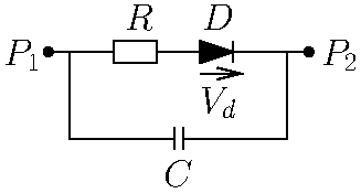
The receiving structure introduced in Fig. 1 is given by a wire frame including two diodes that act as nonlinear loads. The frame is made of perfectly conducting cylindrical wires of cross-section 1 mm. The dimensions of the wire frame are set to 100 mm×100 mm. The incident wave with electric field Einc, magnetic field Hinc, and Poynting vector Sinc carries a transient signal. The polarization of the incident wave is chosen such that the electric field points in y-direction. Electric field components are denoted by Exobs, Eyobs, and Ezobs, recorded by a virtual field probe located at the center of the frame antenna. Simulations of this setup are first performed in the time-domain full wave simulation tool CST Microwave Studio (CST, 2022). The equivalent circuit of the diodes used in the simulations is depicted in Fig. 2. The diode parameters are given in Table 1. These parameters resemble those of a Schottky diode with current voltage relation:
with the Boltzmann constant k and the elementary charge e.
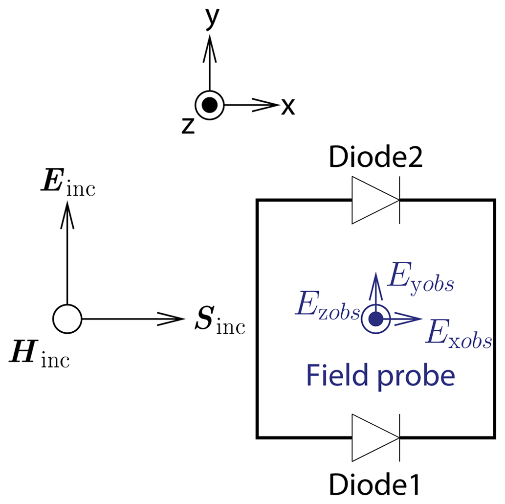
Figure 1Frame antenna with two embedded diodes excited by a plane wave carrying a transient excitation.

2.2 Excitation pulse
As transient HPEM excitation signal, a double exponential pulse is used. It is carried by the incident plane wave and mathematically described by
In order to have E0 as peak value, the correction factor K is introduced with
Additionally, the Heaviside function Θ(t)
is included to define E(t) for all times t. A time delay of Δt=2.5 ns is chosen. The values of α and β are calculated from rise and fall times according to:
2.3 Full wave simulation results of the scattered electric field
A full wave simulation is performed with CST Microwave Studio and the electric field measured by the virtual field probe of Fig. 1 is sampled. This leads to the results displayed in Fig. 3.
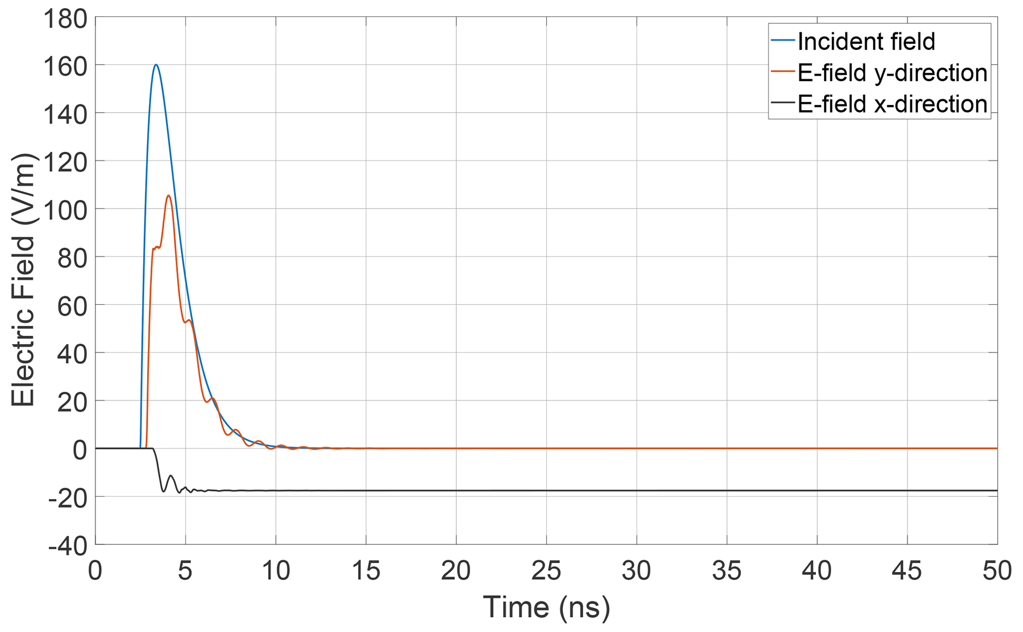
The excitation introduced in Sect. 2.2 is depicted in the figure in blue. Moreover the electric fields in x-direction Exobs and y-direction Eyobs are displayed. It turned out that the electric field at the observation point has no significant component in z-direction. A first observation is that the electric field vector at the observation point includes an x-component that grows rapidly during the passing of the transient excitation and remains approximately constant. The occurence of approximate DC-components caused by the rectifying effect of diodes has already been studied in Michels et al. (2020) for the case of one diode. The novelty in the present simulation is in the time dependency of the field component as it behaves approximately like a Heaviside function without noticeable oscillations. This becomes more clear if this result is compared to the case with a single diode only: In this case, Diode1 in Fig. 1 is replaced by a 40 MΩ resistance which corresponds to the reverse resistance of the diode. The same simulation is repeated leading to the result shown in Fig. 4.

Figure 4Electric fields measured by the virtual field probe for a single nonlinearly loaded receiving structure.
It seems as if in the case of two diodes there is a counteracting effect which leads to a cancellation of initially present oscillation. In the following it will be shown how macromodeling techniques can contribute to calculate and understand this cancellation.
3.1 Basic approach
For the following approach it is an essential idea to replace both diodes by equivalent ideal voltage sources. This is in accordance to the substitution theorem (Maas, 1988). As depicted in Fig. 5, the nonlinearly loaded structure (a) can be decomposed into three separate wire frames including two ideal voltage sources V1 and V2. These wire frames will separately be excited.
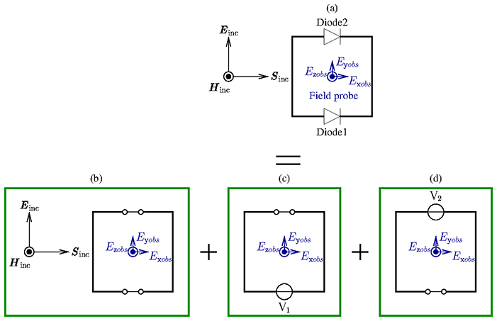
Figure 5Decomposition of the original setup (a) into three configurations (b), (c), and (d).
Since no nonlinear elements are involved in this constellation, the superposition principle can be used to calculate the field strength at the observation point. The field contributions of the three wire frames (b), (c), and (d) are treated separately. The first contribution is caused by the incident field with both voltage sources V1 and V2 set to zero, leading to configuration (b). The other two scattered components are computed by setting alternately one of the voltage sources to zero, leading to the configurations (c) and (d). The field contributions can thus be split into separate parts in order to study their interaction. Before the superposition can be performed, the ideal voltage sources V1(t) and V2(t) corresponding to the voltage drops across the diodes have to be determined.
3.2 Computation of the voltage drops across the diode
It is the aim to create a macromodel of the nonlinearly loaded structure capable to relate the voltage drops V1(t) and V2(t) across the diodes to any excitation signal carried by an incident wave. To do so, the first task is to create a netlist for an electric circuit simulator of the linear part of the structure. For this, the diodes are removed and replaced by ports in a full wave simulation. The scattering parameters of the resulting two-port are computed and provide a set of discrete S-parameters
The continuous functions Sik(s) with are given in the Laplace domain and approximated by a vector fitting algorithm as rational functions in their pole-residue form. For this step a check and enforcement of passivity is mandatory. From the resulting rational functions an equivalent circuit of the structure can be derived with methods explained in Grivet-Talocia and Gustavsen (2016a) and represented by a SPICE netlist. The nonlinear loads are now added in the netlist of an electric circuit simulation as depicted in Fig. 6. We assume that the equivalent circuit represented by the SPICE netlist and the diodes does not contain any electrical or magnetic energy at the initial state. The task to transfer diode parameters from full wave simulation, as introduced in Table 1, for example, into a SPICE netlist or vice versa may not be trivial. Corresponding approaches can be inferred from Chang (1996).
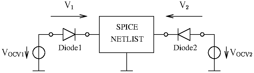
In order to perform the required circuit simulation, the open circuit voltages VOCV1 and VOCV2 have to be computed as well. A model is needed to relate the signal carried by the plane wave to the open circuit voltages.
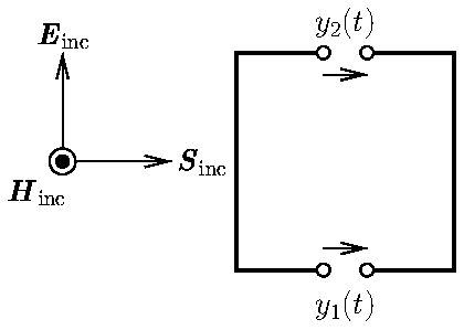
To numerically obtain a suitable model, a time domain full wave simulation of the setup depicted in Fig. 7 is performed with a broadband signal u(t) which leads to the open circuit voltages y1(t) and y2(t). Then a Fourier transformation is applied to these signals, leading to the transforms U(s), Y1(s) and Y2(s). These are given in sampled form such that discrete values of the transfer functions are obtained,
With known discrete values of the transfer function, a vector fitting algorithm is applied to provide a continuous transfer function with residues rk and poles pk. In addition, the propagation time of the plane wave is taken into account by a parameter τ. In this case, only a forward evaluation is required. Therefore a check or enforcement of passivity is not necessary (Wendt et al., 2020) and the desired transfer functions are of the form
Having the transfer functions H1(s) and H2(s) at hand, the open circuit voltages can be calculated for any signal u(t) carried by the incident plane wave via fast recursive convolution with the inverse Fourier transformation of the transfer function h(t) as kernel,
In order to ensure causality of the system the following has to apply for the impulse responses h(t):
The fast recursive convolution method turns out to be very efficient for the case when u(t) is given as input function in time domain and the transfer functions Hn(s) are given in frequency domain in their pole residue form Eq. (8). Further details on the recursive convolution method are provided in Grivet-Talocia and Gustavsen (2016a).
After having determined the open circuit voltages, the electric circuit simulation of the model depicted in Fig. 6 can be carried out. This yields the desired voltage drops V1(t) and V2(t) across the diodes.
3.3 Computation of the electric field at the observation point
The resulting electric field at the observation point is calculated from the decomposition depicted in Fig. 5. In analogy to the methods described in the previous Sect. 3.2, transfer functions are derived for the computation of the electric field at the observation point, caused by the incident field and the voltages V1(t) and V2(t). In total, for the calculation of the observed electric field the following transfer functions are required:
-
Two transfer functions that relate the signal carried by the incoming plane wave to the field components Exobs and Eyobs with
-
Two transfer functions that relate the voltage V1(t) to the field components Exobs and Eyobs with V2(t)=0
-
Two transfer functions that relate the voltage V2(t) to the field components Exobs and Eyobs with V1(t)=0
The fast recursive convolution method is used again to compute the electric field components of Eobs. Finally, the field at the observation point is calculated by summing up the field contributions of the configurations (b), (c), and (d) as shown in Fig. 5.
As a result, the macromodel of the structure introduced in Fig. 1 is now complete and it is possible to compute the electric field at the observation point for any type of excitation signal which is carried by the incident electric field. This also allows to provide a better understanding regarding the interaction of the nonlinear loads, as will be shown in the following.
In order to verify the efficiency of the macromodel, simulation results obtained from both full wave simulations and macromodel simulations are compared. The structure introduced in Sect. 2.1 serves as test setup. Again, it is excited by a plane wave as depicted in Fig. 1 and carries the signal described in Sect. 2.2. The simulation results are displayed in Figs. 8 and 9.
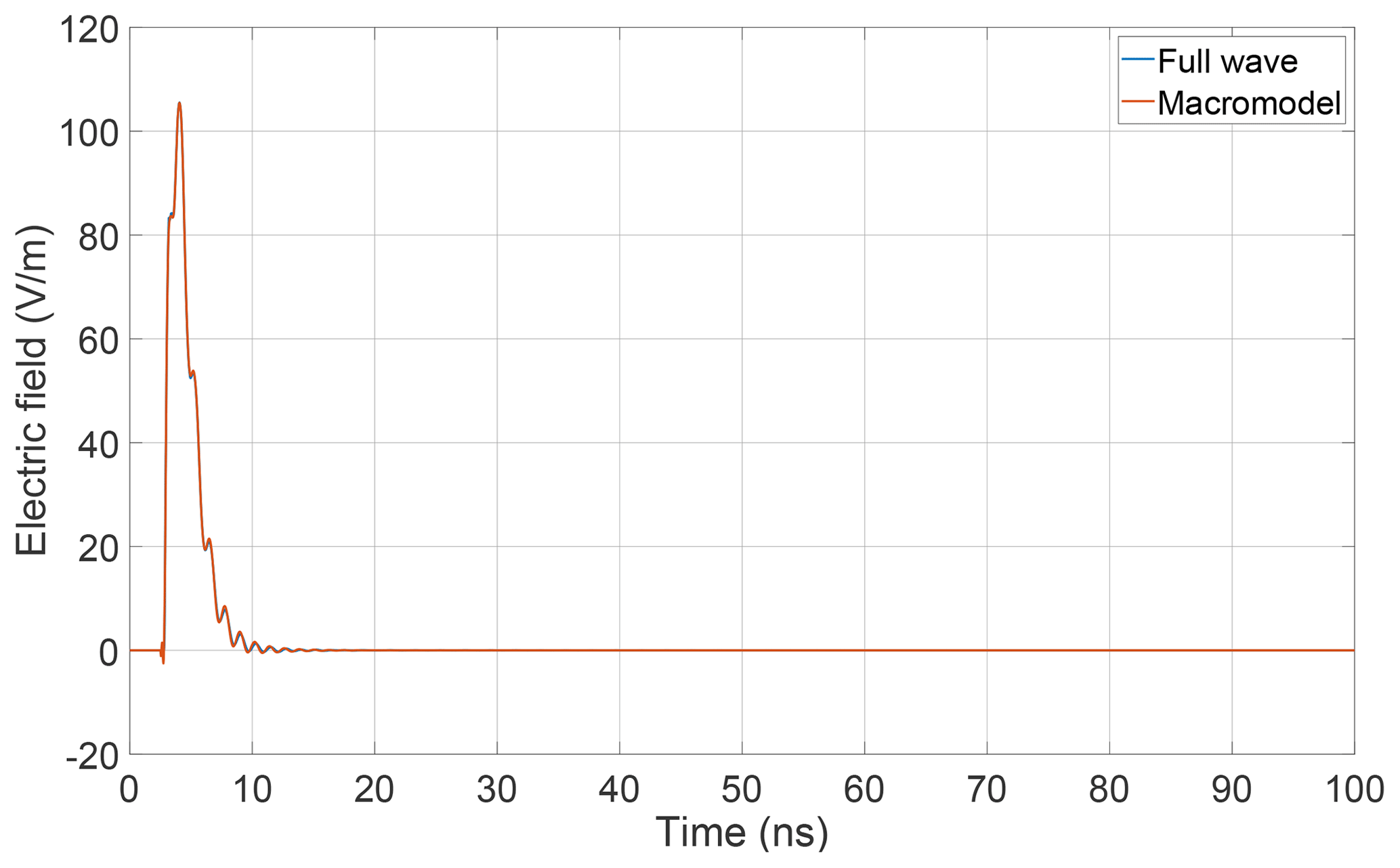
The field component in y-direction, compare also Fig. 1, is reproduced by both the macromodel and the full wave simulations and both methods provide a very good agreement. In view of the different field contributions shown in Fig. 5 this field component is due to configuration (b).
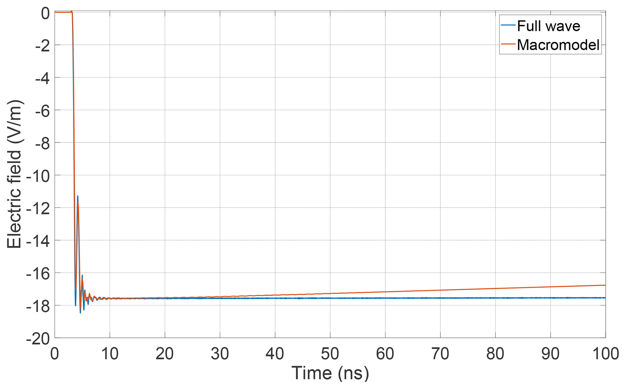
The comparison concerning the field in x-direction shows a satisfying correlation. Deviations are due to the fact that it is difficult to incorporate the diode parameters of Table 1 into an adequate SPICE netlist. Nevertheless, the pronounced DC-component component is reproduced and there is a good match for early times. It turns out that the x-component results from contributions of the configurations (c) and (d).
One question that was raised during the beginning of this investigation was for the reason of the absence of pronounced oscillations in the early time response for the case of two diodes in the antenna. This behavior can now be understood by considering the separate field contributions resulting from the configurations (c) and (d). In Fig. 10 it is revealed that the corresponding DC-components add up while the AC-components cancel out. The sum of both components lead to the time dependency that also is obtained from the full wave simulation.
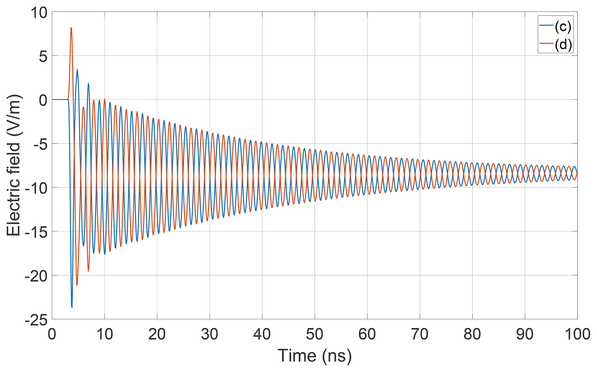
Figure 10x-components of the electric field at the observation point, considered separately for both configurations (c) and (d).
The particular example of a multiple nonlinearly loaded receiving structure showed that macromodeling techniques are an efficient analytical tool. The major advantage is that full wave simulations can be replaced by electric circuit simulations which are much faster and less memory consuming. It is possible to split a complex problem into several parts. Moreover, components with nonlinear characteristics are quite easy to implement in electric circuit simulations. The task to translate data from datasheets of given components correctly into lumped element parameters capable to be used in full wave simulation is not immediate.
As already discovered in former studies, nonlinear loads can lead to DC-components which may persist for a comparatively long time. The interaction of multiple nonlinear loads leads to further effects that a priori are difficult to predict. Methods to investigate these effects in depth are therefore a useful instrument with potential applications to EMC.
The data presented in this article are available from the authors upon request.
The computer simulations and data processing including all graphical representations were carried out by RM. Editorial hints as well as mathematical and physical suggestions were given by MS, SF, and FG.
At least one of the (co-)authors is a member of the editorial board of Advances in Radio Science. The peer-review process was guided by an independent editor, and the authors also have no other competing interests to declare
Publisher’s note: Copernicus Publications remains neutral with regard to jurisdictional claims in published maps and institutional affiliations.
This article is part of the special issue “Kleinheubacher Berichte 2021”.
The authors are indebted to Cheng Yang and Christian Schuster for kindly introducing them to advanced macromodeling techniques.
This research work was partially funded by the Bundeswehr Research Institute for Protective Technologies and CBRN Protection, Munster (grant no. E/E590/JZ001/HF063).
This paper was edited by Alexander Kraus and reviewed by Heyno Garbe and one anonymous referee.
Chang, F.-Y.: Transient Analysis of Diode Switching Circuits Including Charge Storage Effect, IEEE T. Circuits-I, 43, 177–190, https://doi.org/10.1109/81.486442, 1996. a
CST: CST Studio Suite 2017, Dassault Systems, http://www.3ds.com, last access: 7 February 2022. a, b
Grivet-Talocia, S. and Gustavsen, B.: Passive Macromodeling Theory and Applications, 1st edn., edited by: Chang, K., Wiley, ISBN 978-1-118-09491-4, 2016a. a, b, c
Grivet-Talocia, S. and Gustavsen, B.: Black-box Macromodeling and its EMC Application, IEEE Electromag. Compat. Mag., 5, 71–78, https://doi.org/10.1109/MEMC.0.7764255, 2016b. a
Maas, S. A.: Nonlinear Microwave Circuits, 1st edn., Artech House, ISBN 0-89006-251-X, 1988. a, b, c, d
Michels, R., Kreitlow, M., Bausen, A., Dietrich, C., and Gronwald, F.: Modeling and Verification of a Parasitic Nonlinear Energy Storage Effect Due To High-Power Electromagnetic Excitation, IEEE. Trans. Electromag. Compat., 62, 2468–2475, https://doi.org/10.1109/TEMC.2020.2980976, 2020. a, b
Ramo, S., Whinnery, J. R., and Van Duzer, T.: Fields and Waves in Communication Electronics, 3rd edn., Wiley, New York, ISBN 978-81-265-1525-7, 1994. a
Sarkar, T. K. and Weiner, D.: Scattering Analysis of Nonlinearly Loaded Antennas, IEEE Trans. Antennas Porpagat., 24, 125–131, https://doi.org/10.1109/TAP.1976.1141327, 1976. a
Wendt, T., Yang, C., Schuster, C., and Grivet Talocia, S.: Numerical Complexity Study of Solving Hybrid Multiport Field-Circuit Problems for Diode Grids, Int. Conf. Electromagn. Adv. App. (ICEAA), Granada, Spain, 9–13 September 2019, https://doi.org/10.1109/ICEAA.2019.8879021, 2019. a
Wendt, T., Yang, C., Brüns, H. D., Grivet-Talocia, S., and Schuster, C.: A Macromodeling-Based Hybrid Method for the Computation of Transient Electromagnetic Fields Scatterd by Nonlinearly Loaded Metal Structures, IEEE Trans. Electromagn. Compat., 62, 1098–1110, https://doi.org/10.1109/TEMC.2020.2991455, 2020. a
Yang, C., Brüns, H.-D., Liu, P., and Schuster, C.: Impulse Response Optimization of a Band-Limited Frequency Data for Hybrid Field-Circuit Simulation of Large-Scale Energy-Selective Diode Grids, IEEE Trans. Electromag. Compat., 58, 1072–1080, https://doi.org/10.1109/TEMC.2016.2540921, 2016. a
Yang, C., Wendt, T., De Stefano, M., Kopf, M., Becker, C. M., Grivet-Talocia, S., and Schuster, C.: Analysis and Optimization of Nonlinear Diode Grids for Shielding of Enclosures with Apertures, IEEE Trans. Electromag. Compat., 63, 1884–1895, https://doi.org/10.1109/TEMC.2021.3073106, 2021. a
- Abstract
- Introduction
- Full wave simulation of a receiving structure with multiple nonlinear loads
- Macromodel of the simulation setup
- Comparison between full wave and macromodel simulation results
- Conclusions
- Data availability
- Author contributions
- Competing interests
- Disclaimer
- Special issue statement
- Acknowledgements
- Financial support
- Review statement
- References