 | 01 Dec 2023
Generating AI modules for decoupling capacitor placement using simulation
Nima Ghafarian Shoaee
Zouhair Nezhi
Werner John
Ralf Brüning
Jürgen Götze
The effects of parameters affecting the input impedance of a power delivery network (PDN) are investigated. It is considered that the size of the power plane and the number of associated planes in the PCB layout, apart from the decoupling capacitor, have an effect on the impedance behavior within a certain frequency range. An artificial neural network (ANN) is trained using the generated data utilizing a process to generate suitable input for training a machine learning (ML) module, which is able to predict the impedance profile of the PDN. In order to obtain a more accurate prediction, Bayesian optimization is implemented and the results are compared to commercial power integrity (PI) software.
- Article
(657 KB) - Full-text XML
- BibTeX
- EndNote


Developing a reliable PDN that provides a constant power supply for integrated circuits (IC) has become more critical with the increase in both operating frequencies and current loads in modern high-performance computing systems. Its importance does not appear to be shrinking given the continuing trends toward system integration and supply voltage reduction. Therefore, PI analysis is an essential part of PDN design of electronic systems. Typically, the performance of a PDN is evaluated based on its impedance response as a function of operating frequency. This is then compared to a target impedance (TI) to determine if the PDN is performing sufficiently well. The exact solution of this problem is usually very time consuming and it requires a lot of experience to obtain a reasonable PDN design in the layout process of the printed circuit board (PCB).
In recent years, an alternative way to achieve an accurate and optimized design of PDN that does not violate the TI, in the academic as well as in the industrial field, are artificial intelligence (AI) methods that have made it possible to redesign and optimize the design with little effort in time. The approach of Schierholz et al. (2019) illustrates the prediction of TI violation with ANN using a simple board design with respect to decoupling capacitors (decaps) placement. A deep learning approach is proposed by Zhang et al. (2021), where a boundary element method (BEM) is used to predict the impedance of the arbitrary irregular generated board. Within a prototype EDA tool package, Choy et al. (2023) implement deep learning-based real-time impedance prediction and optimization of decap selection and placement. In Han et al. (2022), another approach based on reinforcement learning is presented for power plane optimization in PDN. A method for selecting both, decaps and their placement concurrently is proposed in Han et al. (2021).
However for all the above methods either multiple full-wave/PI simulations are required throughout the optimization process, making the whole process time-consuming, or non-physics-based methods are used to calculate impedance at each iteration, resulting in a lack of accuracy in real PCB design.
In Na et al. (2000), an analytical formulation for modeling a plane-pair structure is presented, as well as an extension for multiple plane pairs that calculates the impedance matrix at arbitrary ports in the plane. Therefore, in addition to the decaps, the number of associated planes in the PCB structure and the size of the power plane have an impact on the impedance behavior in a given frequency range. This important impact can also be expected from the AI modules supporting the design process. Using two case studies this is verified in the present paper.
In this paper, we present an approach that generates data for developing an ANN that not only considers the decaps, but also incorporates the structure of multiple layers and the size of the power plane in the development of PDN. These data are then used to train an ANN and the prediction accuracy will be compared to simulated one.
Several parameters are involved in the design of a PDN. A variation of these parameters, the resulting impedance response can violate the TI. We will focus on three main cases and perform simulations using the accurate PI simulator eCADSTAR (ZUKEN, 2022) to discuss the effects of these parameters on the impedance response.
The first and primary parameter that fixes the PI problem is to work with decoupling capacitors. The number of associated decaps on the PCB and their position must be well defined to satisfy the PI criterion. A decap can theoretically (under optimal operating conditions) be treated as a bare capacitor with purely capacitive properties, however, in the real design, a capacitor also has some resistive (Equivalent Series Resistance) and inductive (Equivalent Series Inductance) properties associated with it, which are known to as parasitic resistance or parasitic inductance (Ott, 2009; Franz, 2013). These characteristics cause a different frequency behaviors and can shift the resonance point of the different capacitors. Therefore, the values of the associated decaps on PDN efficiency must be taken into account. Practical experience and simulation experiments do indicate, that the closer the decaps are placed to the observation point, the greater the influence on the resulting impedance response.
Two other parameters that must be considered are the size of the power plane and the number of layers in a PCB technology. Analytical formulas for calculating the impedance matrix of a solid plane pair and its extension to multiple planes are presented in relations (4) and (16) of Na et al. (2000). The detailed derivation of these formulas is clearly explained in this paper. Based on these relations, modifying the dimensions of the plane and the total number of associated ground planes changes the impedance characteristics. Since the electrical properties (relative permittivity, conductivity, and loss factor) are considered as fixed in the design process. Besides the placement of the decaps and their values, the study of the PCB stackup and plane dimensions (power/ground) are also relevant for the design purpose. The change in impedance characteristics requires, therefore, a systematic analysis of the influence of the above parameters on the PDN.
To reduce the complexity of the problem, we consider the above parameters separately. Therefore, we have defined two case studies in which the effects of decaps and the stackup definition are treated independently. These are described in Sect. 3.1 and 3.2.
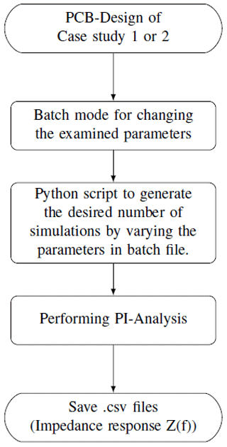
In the previous section, the most common and important parameters in the design of a PDN were discussed. To use this knowledge to build and evaluate an ML module capable of predicting the impedance curve of a PDN system, some data is needed to train and test ML algorithm. To perform this task correctly and automatically, we define a workflow as shown in Fig. 1. First, we design a PCB in eCADSTAR PCB Editor and then a batch script to change the parameters to be analyzed. After that, depending on how much data is needed, a Python script generates these batch scripts in a repeated process. Then the simulations are performed in eCADSTAR PI/EMI Analysis and the impedance data of the simulations are saved as different CSV files. Based on this workflow and the definition of the following case studies, the data sets are generated.
3.1 Case study 1
In this case study, the effect of the decaps is investigated. Not only the number of involved decaps but also the position of the decaps in relation to the IC power pin investigated. For this purpose, an irregular H-shaped board with dimension of 300×320 mm2 (W×H) as shown in Fig. 2 was designed with four layers technology (two layers as top and bottom, one as power and the other as ground) and one IC. The decaps can be positioned in the defined grid on the board (the assigned positions 1 to 52 in Fig. 2). As described in Sect. 2, the position of the decaps is important in relation to the position of the IC. Therefore, we investigated three areas where the decaps have been placed randomly:
-
up to 10 decaps with random distribution at predefined positions on the corners of the board (area 1),
-
up to 10 decaps with random distribution at predefined positions around the IC of interest (area 2),
-
and finally up to 10 decaps are distributed at the 52 predefined positions on the entire top layer of the PCB randomly (area 3).
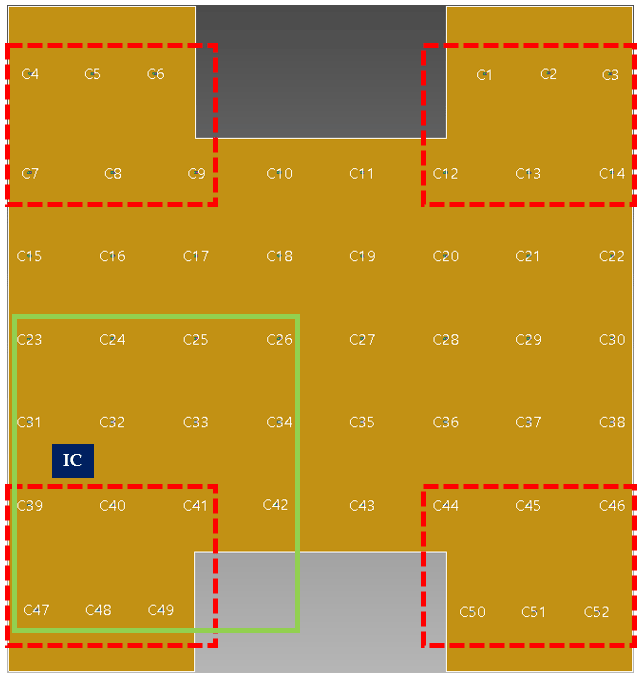
Figure 2Test board of case study 1: randomly distributed decaps at the corners of the board (red-dashed rectangle) as area 1 and random distribution of decaps around the IC position (green-solid rectangle) as area 2. The numbered positions from 1 to 52 are used for placing the decaps.
The positioning of the decaps and their types is as described in Table 1 and Fig. 4 of Cecchetti et al. (2020). Three types of capacitors coded as 1, 2 and 3 with corresponding values for C, ESL and ESR are:
-
Type1 (100 nF, 222 pH, 8.9 mΩ)
-
Type2 (47 nF, 154 pH, 21.4 mΩ)
-
Type3 (22 nF, 142 pH, 25.2 mΩ).
To determine the placement of the decaps on the board, the following vector d1 of size 1 by 20 is used for each simulation depending on the number of added decaps and their type:
where Pk is the position of the decap on the board and Tj is the respective type of decap. Thus, up to 10 decaps with 3 different types could be placed randomly on the board.
3.2 Case study 2
As discussed in Sect. 2, the board structure and the effect of varying size of the power supply plane are of interest in the PDN design process. To look at these parameters in more detail, a simple square board with overall dimensions of 200×200 mm2 and an IC in the center is considered. Figure 3 shows the test board and its stackup.
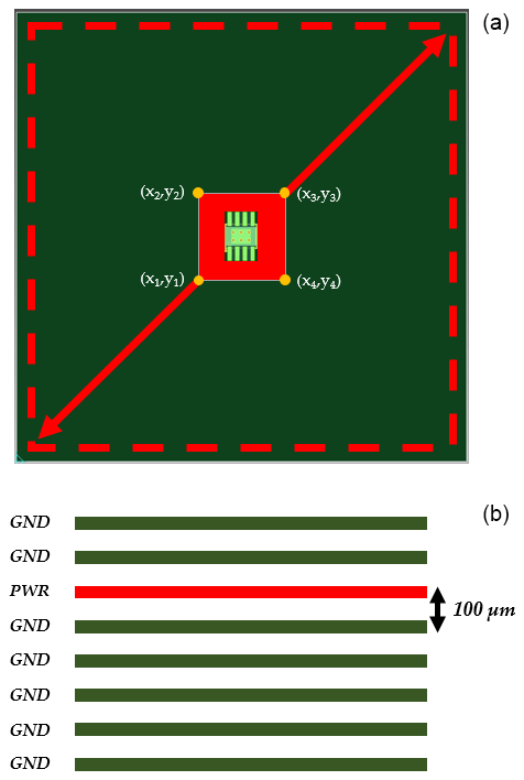
Figure 3Test board of case study 2: Top view of the simulated PCB (a) and its stackup (b). The size of the PWR plane (red plane), its position in the PCB structure and the number of GND planes vary in this case study.
To create different simulations for various stackup and power plane sizes, we define the following vector d2 of size 1 by 16:
where the first 8 elements define the edges of the power plane, which are changed in 1 mm grid. The second 8 elements describe the type of plane, coded as 1 for GND, 2 for PWR and 0 if no plane is to be considered .
A suitable method to approximate a function on a bounded domain with a certain degree of accuracy is an ANN which is defined by its layers (including input, some hidden layers, and output) and neurons. The general structure of an ANN is shown in Fig. 4. The ANN is implemented by using the toolkits scikit-learn (Pedregosa et al., 2011) and TensorFlow (Abadi et al., 2015) using Adam optimizer (Kingma and Ba, 2014).
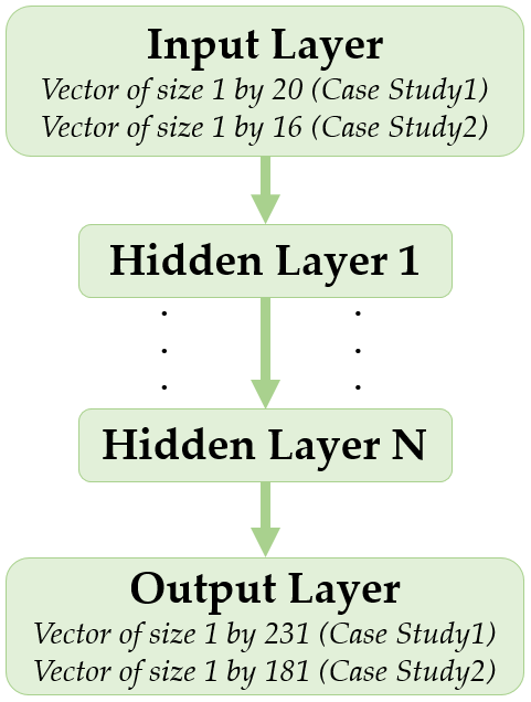
Figure 4Artificial Neural Network (ANN) structure with input, hidden and output layers. Depending on the case study, the normalized input feature may be different.
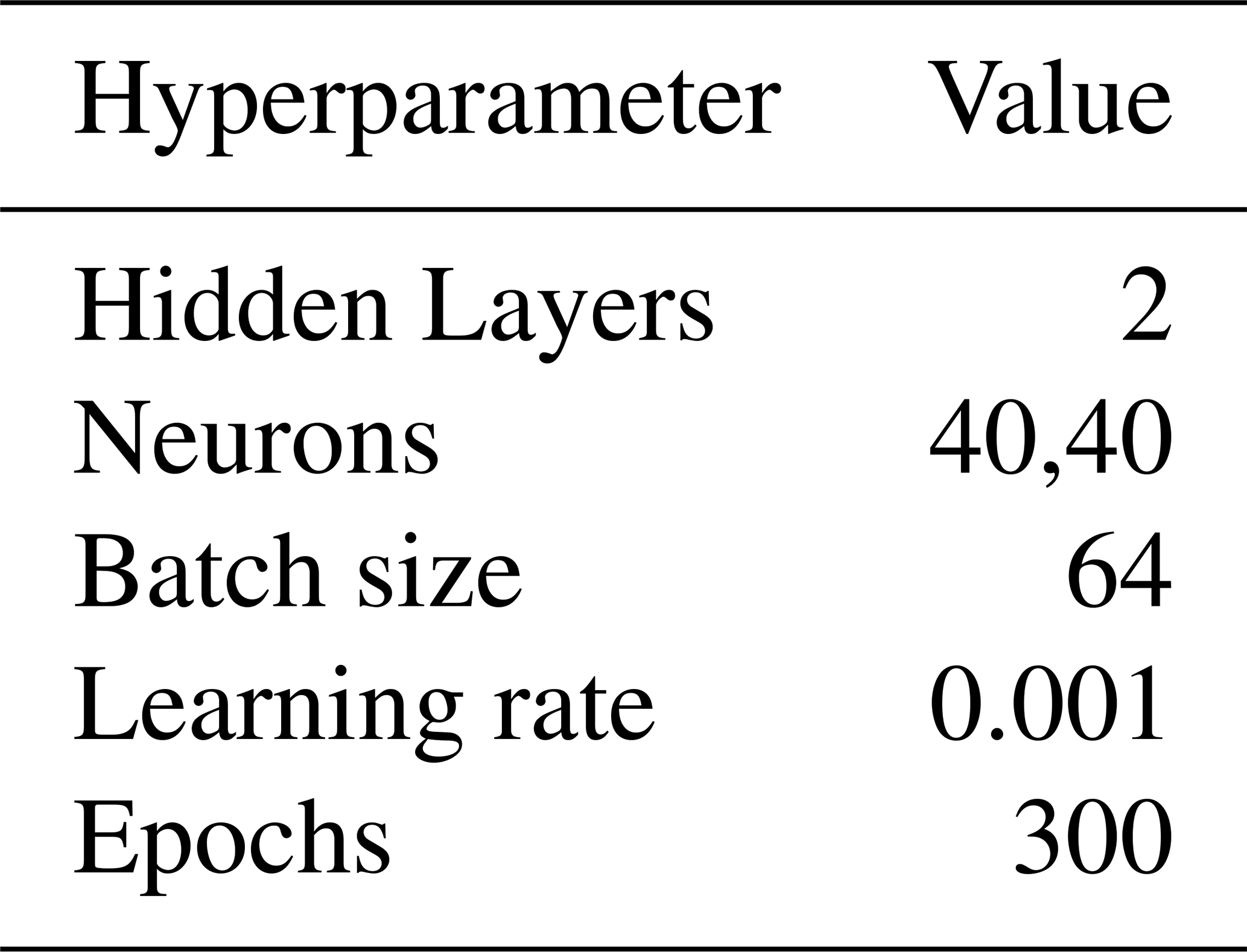
Based on the procedure in Fig. 1 and the input vector d1 for case study 1, 5001 simulations are created as a training data set for each predefined area of case study 1. The performance of the training is increased by performing a min-max normalization of the data for the input and output layers (feature scaling). All simulations are performed with 231 logarithmically distributed points in the frequency range from 1 to 600 MHz. 80 % of the data is used as training data, and the remaining part is divided equally as test and validation data. Then, an ANN is trained with the hyperparameters listed in Table 1.
The mean square error (MSE) is calculated as follows to determine the accuracy of the trained network:
where N, , and yi represent the number of data points, predicted value, and actual value, respectively. The best MSE results of the test data for each of the areas are indicated as follows: MSEarea1=1.31, MSEarea2=0.7 and MSEarea3=1.28.
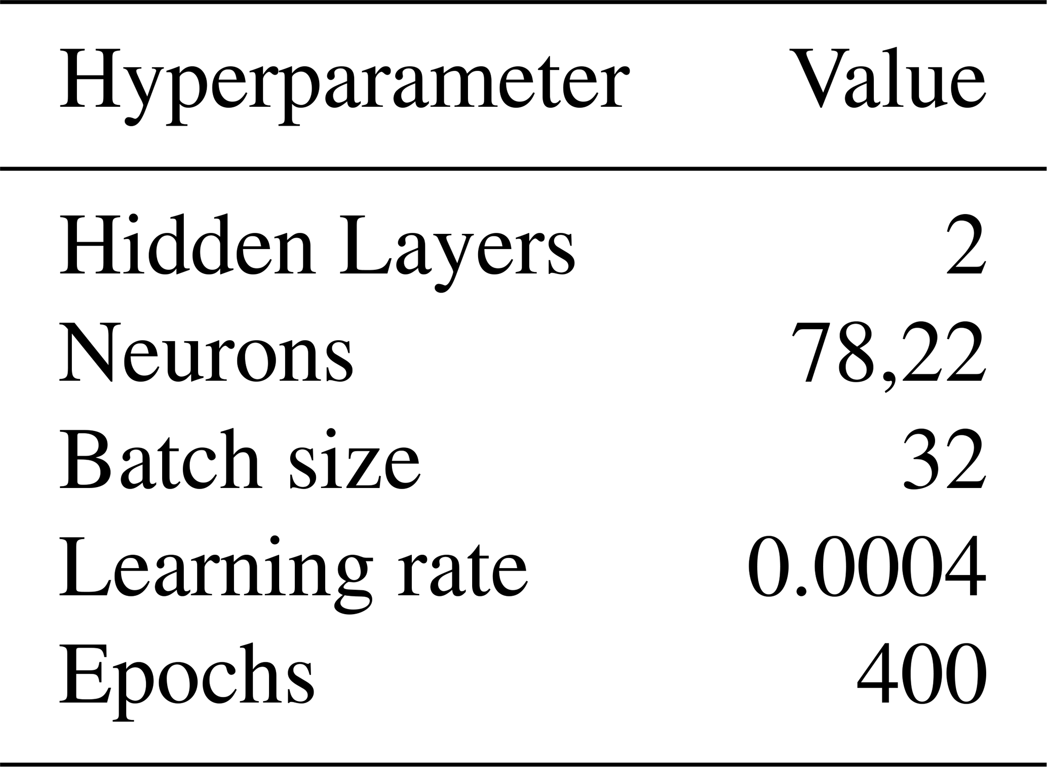
For case study 2, by varying the number of layers, size and position of the power plane in the board structure, 51 840 data samples are generated in the frequency range of 100 MHz to 1 GHz (since no decap is involved in the design, this frequency range is the one where the planes will affect the impedance response) with 181 logarithmically distributed points. The neural network hyperparameters are as shown in Table 2. The best MSE was calculated as 0.29 this time.
Figures 5 and 6 show the predicted impedance response compared to the simulated one from a sample of the test data in case study 1 and 2, respectively. For both cases, the data shows acceptable prediction of the impedance curve with a expected impedance profile. The ANN output agrees well with the capacitive response of the board at low frequencies, below the first resonance (about 7.6 MHz in case study 1 and 210 MHz in case study 2). Beyond this resonance, the inductive impedance profile is also well predictable.
It is important to mention that the ANN-hyperparameters used in this section are the optimized ones. The process of hyperparameter tuning is explained in the next section.
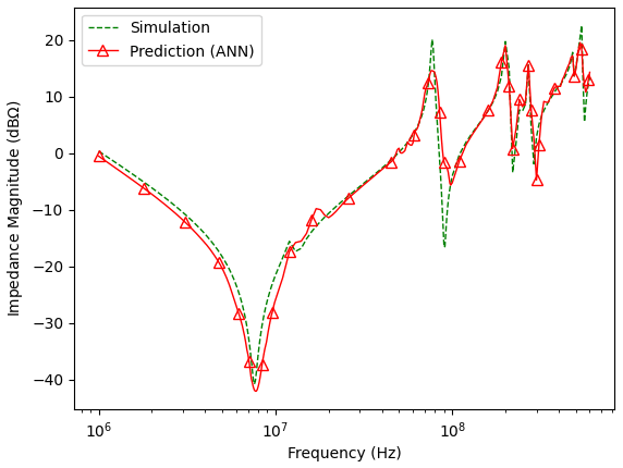
Figure 5Comparison of the ANN prediction in case study 1 and the impedance simulation results for a sample from the test dataset.
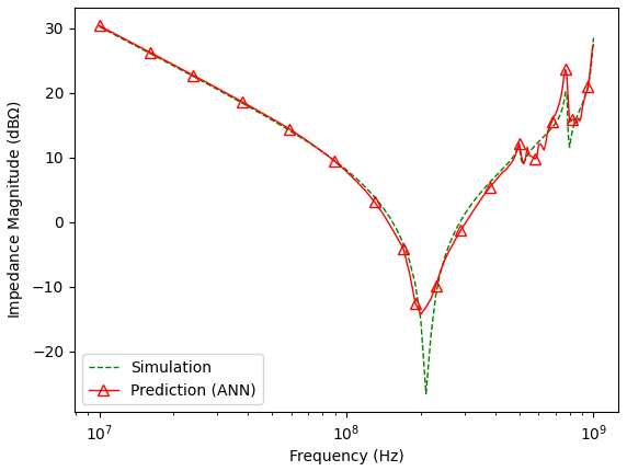
Figure 6Comparison of the ANN prediction in case study 2 and the impedance simulation results for a sample from the test dataset.
Impact of hyperparameter tuning on prediction quality
It is not straightforward to figure out the structure of an ANN depending on its application. For example, the choice of the number of hidden layers and neurons on each of them, as well as some other parameters such as learning rate, batch size, activation function, etc., may affect the fitting quality. The consequence is that decreasing or increasing the number of layers and neurons may decrease the fitting performance of the ANN or cause an overfitting problem. In particular, an unfavorable number of layers and neurons may lead to larger error or unacceptable prediction of the ANN output. For this reason, we have tried to find an optimal or at least semi-optimal solution to select the best possible hyperparameter values to achieve a good prediction of the impedance curves. Among several methods to perform this task in the Python environment we obtained the optimal hyperparameters by implementing Bayesian Optimization (BO) tuning using Keras (Chollet, 2015).
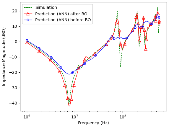
Figure 7Plot of the impact of Bayesian optimization on prediction accuracy for a sample of test data in Case Study 1 compared to the accurate simulation results. The blue curve shows the ANN output before hyperparameter optimization when the initial ANN parameters are not well chosen. In contrast, the red curve shows the optimized ANN output where curve profile and peak amplitude are acceptably predicted.
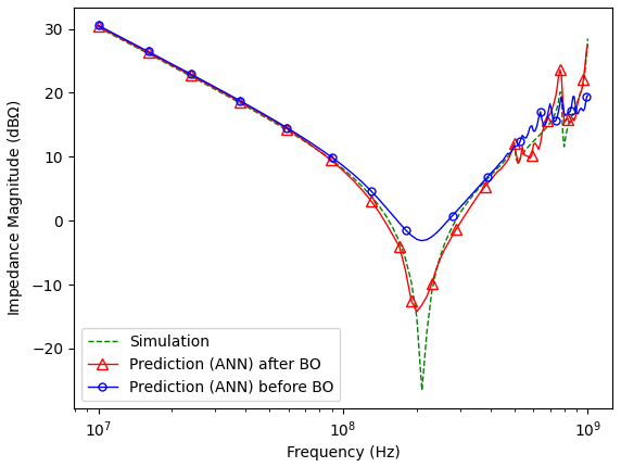
Figure 8Plot of the impact of Bayesian optimization on prediction accuracy for a sample of test data in Case Study 2 compared to the accurate simulation results. The blue curve shows the ANN output before hyperparameter optimization when the initial ANN parameters are not well chosen. In contrast, the red curve shows the optimized ANN output where curve profile and peak amplitude are much better predicted.
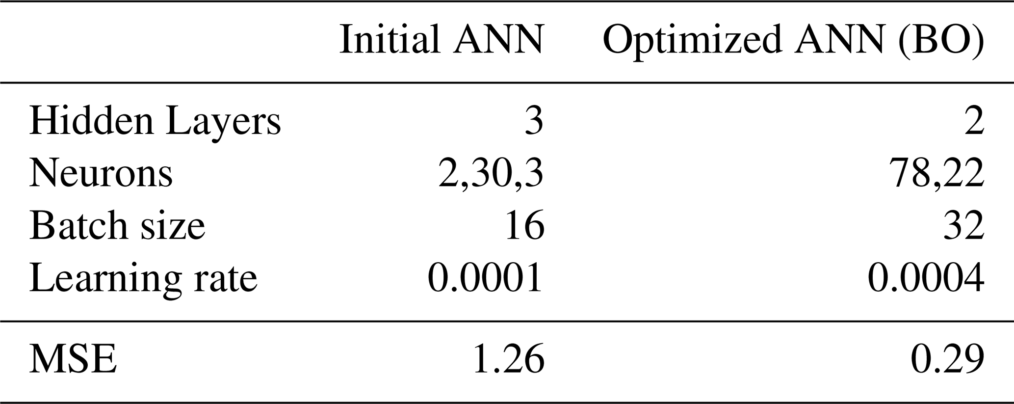
For both boards under examination, the effect of BO is determined. We started with an ANN with 3 hidden layers and 2 neurons in the first and third layers and 30 neurons in the second layer. The batch size = 16 and learning rate = 0.001 have been set for both cases. The MSE values for the first and second cases are calculated as 1.37 and 1.26, respectively. After implementing BO, the new MSE values are 0.7 and 0.29 for case 1 and case 2, respectively. In Tables 3 and 4, the hyperparameter tuning results for both cases are merged for comparison with the case without BO. The illustration of the comparison of the initial ANN and with BO tuned ANN is shown in Figs. 7 and 8 for case study 1 and 2, respectively.
Table 3Comparison of the ANN hyperparameters before and after BO and the resulting MSE in case study 1.
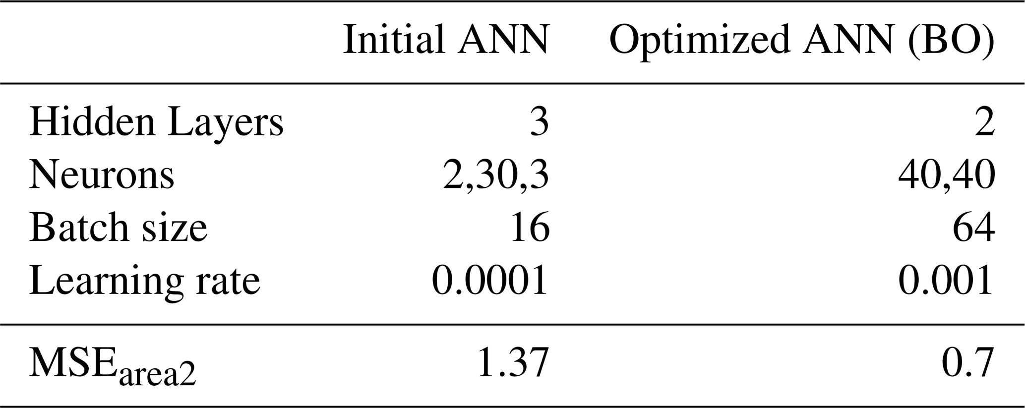
Table 4Comparison of the ANN hyperparameters before and after BO and the resulting MSE in case study 2.
To evaluate the performance and predict the input impedance of a PDN, a process for training and evaluating ML modules with respect to various parameters (decap values and their positions, PCB multilayer structure, various power plane sizes) has been developed. The impedance curve predicted by ANN matches well with the curve simulated by commercial PI software if suitable ANN hyperparameters are chosen. To achieve good results, BO tuning offers a fast and accurate way to obtain a well-trained module capable of predicting the resonance points and inductive trend of the impedance profile with acceptable accuracy. Although its accuracy does not match completely full-wave or other numerical PI simulators, the trained ANN is a significantly faster method compared to commercial PDN software when one wants to perform an optimization process, which needs the impedance response calculation on each iteration. The results obtained in this work indicate a good possibility to perform optimization methods to improve and support PDN designs. One of these methods is the genetic algorithm (GA). In another paper, this process is published in detail based on the results of the current paper (Nezhi et al., 2023). Also, the involvement of reinforcement learning could increase the capability of optimization and the accuracy of the supported PDN designs. Transfer learning and physics-informed ML will be considered in our future work to improve the applicability of ML methods in the slight modification of PCB structure.
Due to project restrictions, the source codes and datasets are not publicly available. For more information, please contact the main author.
NGS developed the concept for this part of the research topic PI-appropriate design. NGS developed and implemented the ANN models and the training the training methods. In addition, NGS developed and implemented the data generation procedures. NGS wrote the initial and final manuscript. ZN supported the programming of ANN models. WJ contributed to the understanding of the PI knowledge domain and the evaluation of PI prediction results. In addition, he supervised the overall research process in the progressiveKI project (UseCase#1: (PDN Design (PCB))) and partially contributed to the improvement of the manuscript. RB supported the development of AI models by providing appropriate data sets and understanding the perspective of PCB designers at terms of practical PDN design requirements and the application of PI design rules. RB also supported the efficient use of the ZUKEN eCADSTAR PI design environment in the context of the progressiveKI UseCase#1 (PDN Design (PCB)). ZN, WJ, RB, and JG discussed the results, contributed to the final manuscript, and provided editorial input. JG guided the entire research process at TU Dortmund (Information Processing Laboratory) and performed the manuscript review.
The contact author has declared that none of the authors has any competing interests.
The responsibility for this publication is held by the authors only.
Publisher's note: Copernicus Publications remains neutral with regard to jurisdictional claims in published maps and institutional affiliations.
This article is part of the special issue “Kleinheubacher Berichte 2022”. It is a result of the Kleinheubacher Tagung 2022, Miltenberg, Germany, 27–29 September 2022.
This work is funded as part of the research project progressivKI (https://www.edacentrum.de/projekte/progressivKI, last access: 12 September 2023) in the funding program NFST by the Bundesministerium für Wirtschaft und Klimaschutz (BMWK) of the Federal Republic of Germany (grant no. 19A21006O/R/B).
This paper was edited by Thomas Kleine-Ostmann and reviewed by two anonymous referees.
Abadi, M., Agarwal, A., Barham, P., Brevdo, E., Chen, Z., Citro, C., Corrado, G. S., Davis, A., Dean, J., Devin, M., Ghemawat, S., Goodfellow, I., Harp, A., Irving, G.,Isard, M., Jozefowicz, R., Jia, Y., Kaiser, L., Kudlur, M., Levenberg, J., Mané, D., Schuster, M., Monga, R., Moore, S., Murray, D., Olah, C., Shlens, J., Steiner, B., Sutskever, I., Talwar, K., Tucker, P., Vanhoucke, V., Vasudevan, V., Viégas, F., Vinyals, O., Warden, P., Wattenberg, M., Wicke, M., Yu, Y., and Zheng, X.: TensorFlow: Large-Scale Machine Learning on Heterogeneous Systems, https://www.tensorflow.org/ (last access: 12 September 2023), 2015. a
Cecchetti, R., de Paulis, F., Olivieri, C., Orlandi, A., and Buecker, M.: Effective PCB Decoupling Optimization by Combining an Iterative Genetic Algorithm and Machine Learning, Electronics, 9, 1243, https://doi.org/10.3390/electronics9081243, 2020. a
Chollet, F.: Keras, https://github.com/fchollet/keras (last access: 12 September 2023), 2015. a
Choy, D., Bartels, T., Stube, B., and Bruening, R.: A Contribution to the Treatment of Power Integrity Design Tasks using Reinforcement Learning, Adv. Radio Sci., 20, this issue, 2023. a
Franz, J.: EMV, Springer Fachmedien Wiesbaden GmbH, https://doi.org/10.1007/978-3-8348-2211-6, 2013. a
Han, S., Bhatti, O. W., and Swaminathan, M.: Reinforcement Learning for the Optimization of Decoupling Capacitors in Power Delivery Networks, in: 2021 IEEE International Joint EMC/SI/PI and EMC Europe Symposium, 544–548, https://doi.org/10.1109/EMC/SI/PI/EMCEurope52599.2021. 9559342, 2021. a
Han, S., Bhatti, O. W., and Swaminathan, M.: Reinforcement Learning for the Optimization of Power Plane Designs in Power Delivery Networks, in: 2022 IEEE 31st Conference on Electrical Performance of Electronic Packaging and Systems (EPEPS), 1–3, https://doi.org/10.1109/EPEPS53828.2022.9947173, 2022. a
Kingma, D. P. and Ba, J.: Adam: A Method for Stochastic Optimization, http://arxiv.org/abs/1412.6980, Published as a conference paper at the 3rd International Conference for Learning Representations, San Diego, 2015, 2014. a
Na, N., Choi, J., Chun, S., Swaminathan, M., and Srinivasan, J.: Modeling and transient simulation of planes in electronic packages, IEEE T. Adv. Packaging, 23, 340–352, https://doi.org/10.1109/6040.861546, 2000. a, b
Nezhi, Z., Ghafarian Shoaee, N., and Stiemer, M.: Iterative Placement of Decoupling Capacitors using Optimization Algorithms and Machine Learning, Adv. Radio Sci., 20, this issue, 2023. a
Ott, H. W.: Electromagnetic compatibility engineering, Wiley, John Wiley & Sons Inc, ISBN 978-0-470-18930-6, 2009. a
Pedregosa, F., Varoquaux, G., Gramfort, A., Michel, V., Thirion, B., Grisel, O., Blondel, M., Prettenhofer, P., Weiss, R., Dubourg, V., et al.: Scikit-learn: Machine learning in Python, J. Mach. Learn. Res., 12, 2825–2830, 2011. a
Schierholz, C. M., Scharff, K., and Schuster, C.: Evaluation of Neural Networks to Predict Target Impedance Violations of Power Delivery Networks, in: 2019 IEEE 28th Conference on Electrical Performance of Electronic Packaging and Systems (EPEPS), 1–3, https://doi.org/10.1109/EPEPS47316.2019.193225, 2019. a
Zhang, L., Juang, J., Kiguradze, Z., Pu, B., Jin, S., Wu, S., Yang, Z., and Hwang, C.: Fast impedance prediction for power distribution network using deep learning, Int. J. Numer. Model., 35, e2956, https://doi.org/10.1002/jnm.2956, 2021. a
ZUKEN: eCADSTAR, https://www.ecadstar.com/de/ (last access: 12 September 2023), 2022. a