 | 27 Apr 2023
Modeling and Analytical Description of Parasitic Probe Effects in Measurements of Conductor-Backed Coplanar Waveguides
Gia Ngoc Phung
Uwe Arz
On-wafer measurements are of fundamental importance to the characterization of active and passive devices at millimetre-wave frequencies. They have been commonly known to be ambitious and challenging due to the occurrence of parasitic effects originating from probes, multimode propagation, crosstalk between adjacent structures and radiation. While a lot of investigations have been performed for conventional coplanar waveguides (CPW) measured on ceramic chucks, the parasitic effects occuring in conductor-backed CPWs (CB-CPWs) have not been fully understood yet. Therefore, this paper presents a thorough study for CB-CPWs based on electromagnetic simulations. Additionally, this paper proposes an analytical description accounting for the probe geometries to predict the occurrence of resonance effects due to the propagation of the parallel-plate-line (PPL) mode. For the first time, a new analytical description including the effects of the probe geometries is presented and validated by both measurements and simulations.
- Article
(13806 KB) - Full-text XML
- BibTeX
- EndNote


On-wafer measurements have been known as ambitious and challenging as they include several parasitic effects degrading the accuracy of the calibrated results. In recent years, a major effort has been undertaken to clarify the source of parasitic effects on coplanar waveguides performed in the framework of the PlanarCal project (EMPIR, 2023). It has been found that the parasitics are caused by different disturbances such as e.g. multimode propagation, crosstalk effects and the influence of millimeter-wave probes. The influence of surface waves and surface-wave like modes has been investigated for more than two decades (e.g. Tsuji et al., 1992; Shigesawa et al., 1990). In Godshalk (1992) the effect of surface waves in wafer probing environments has been discussed. More recently, the effect of substrate modes on multiline-Thru-Reflect-Line (mTRL) calibrated measurements has been clarified (Phung et al., 2018a) up to 220 GHz and the multimode propagation causing radiation effects has been discussed up to 325 GHz (Spirito et al., 2018b).
Parasitic effects caused by the influence of probes have been investigated thoroughly in conjunction with the impact of neighborhood in the layout (Phung et al., 2019). In Fregonese et al. (2018) a similar investigation has demonstrated the probe effects at higher frequencies and these investigations have been extended up to 500 GHz for different probe topologies (Yadav et al., 2020). In Spirito et al. (2018a) measures how to avoid and mitigate the parasitic effects have been proposed. While a number of investigations have been performed for conventional coplanar waveguides measured on ceramic chucks, the parasitic effects occuring in conductor-backed (CB) CPWs are not yet fully understood. The CB-CPW case is of fundamental importance because it is widely used in many applications for monolithic microwave circuits (MMICs), hybrid integrated circuits and PCBs. CB-CPWs offer several advantages with regard to improved mechanical strength and heat sinking capabilities. However, the presence of a bottom ground plane allows for the propagation of an additional parallel-plate-line mode or microstrip-type mode, a TEM mode which occurs without any cutoff frequency. In McKinzie and Alexopoulos (1992) the leakage behavior of the PPL mode alongside the dominant CPW mode was investigated for CB-CPWs and in Liu and Itoh (1993) for multilayered CB-CPWs. In Lee and Lee (1998) and Amado-Rey et al. (2018) the influence of the PPL mode was investigated for both flip-chip and active devices, discussing the impact of the bottom ground plane in amplifiers. Moreover, measures using via holes to connect the ground were proposed to suppress the propagation of the PPL mode.
All the investigations confirm that the PPL mode has a large impact on the performance of CB-CPW circuits. The PPL mode does not only occur in packaged CB-CPWs or active devices. Whenever CPWs are measured directly on metal chucks, there are electrical potential differences between the conductors residing on top of the substrate and on the bottom ground. Therefore, the PPL mode can already occur during on-wafer characterization of the CPWs and thus have an impact on the resulting measured data. So far, many publications have demonstrated the impact of parasitic probe effects for conventional CPWs. Till now, however, the parasitic probe effects in CB-CPWs are not fully understood, and a thorough study in regard with the probe effects in CB-CPWs is still lacking. With this motivation, the goal of this paper is to close this gap and to clarify the underlying phenomena of the probe influences for CB-CPWs. It does not only present a systematic study, but also proposes an analytical description to predict the occurence of PPL resonance effects in interaction with parasitic probe effects. Starting with a measurement example, this paper presents a systematic study of how the parasitic probe effects deteriorate mTRL-calibrated S-parameters of CB-CPWs (which is an extended work of Phung and Arz, 2021b).
The outline of this paper is described as follows: to demonstrate the parasitic effects in CB-CPWs, the first section presents a comparison between measurements and electromagnetic (EM) simulations of CB-CPWs of different line lengths. The second part shows a systematic study by varying the probe properties. Based on this study, an analytical approach is presented to predict the occurence of the PPL resonance effects taking the probe geometries into consideration. Finally, the analytical description is validated for different substrate materials by fullwave 3D EM simulations (CST, 2020) and verified by measurements.
All simulated and measured data presented here have been processed by applying the mTRL calibration according to Marks (1991). The calibration set consists of a short as reflect, a 400 µm long CPW line as thru and a selection of seven additional lines with lengths between 500 and 11 400 µm. The common parameters of the CPW cross section (which has been used in Arz et al., 2019) are the signal width w = 62 µm, the gap width s = 6 µm, the metal ground width wg = 250 µm and the metal thickness t = 0.534 µm on fused silica substrate (ϵr = 3.78). All the measurements were performed with GGB probes with a 100 µm pitch. The measurements were performed on a metal chuck to emulate the CB-CPW case and additionally on a ceramic chuck to avoid the propagation of PPL mode and surface waves (with a permittivity ϵr,chuck = 6.5 larger than that of the wafer ϵr = 3.78; see Arz et al., 2019; Spirito et al., 2018a). The ceramic case is therefore used in most cases as a reference for comparison. In the electromagnetic simulations, CST from Dassault Systemes was used (CST, 2020). In order to realistically emulate the given scenarios, the layout of the complete wafer with all neighboring effects was modeled (Phung et al., 2019). For the excitation, the sophisticated probe model of Phung et al. (2018b) (taking into account the probe geometry) was applied. The reference plane of the calibration for both chuck conditions was shifted to the probe tips to enable comparisons between simulations and measurements.
The measured and simulated magnitudes of the transmission coefficient S21 of CPWs of different line lengths for both chuck conditions are compared in Figs. 1–4. For comparison purposes the relative difference is plotted, which is defined as follows:
The relative difference is determined for the simulated and measured data according to Eq. (1). The line lengths selected for the comparison are l = 11 400, 5400, 2400 and 900 µm.
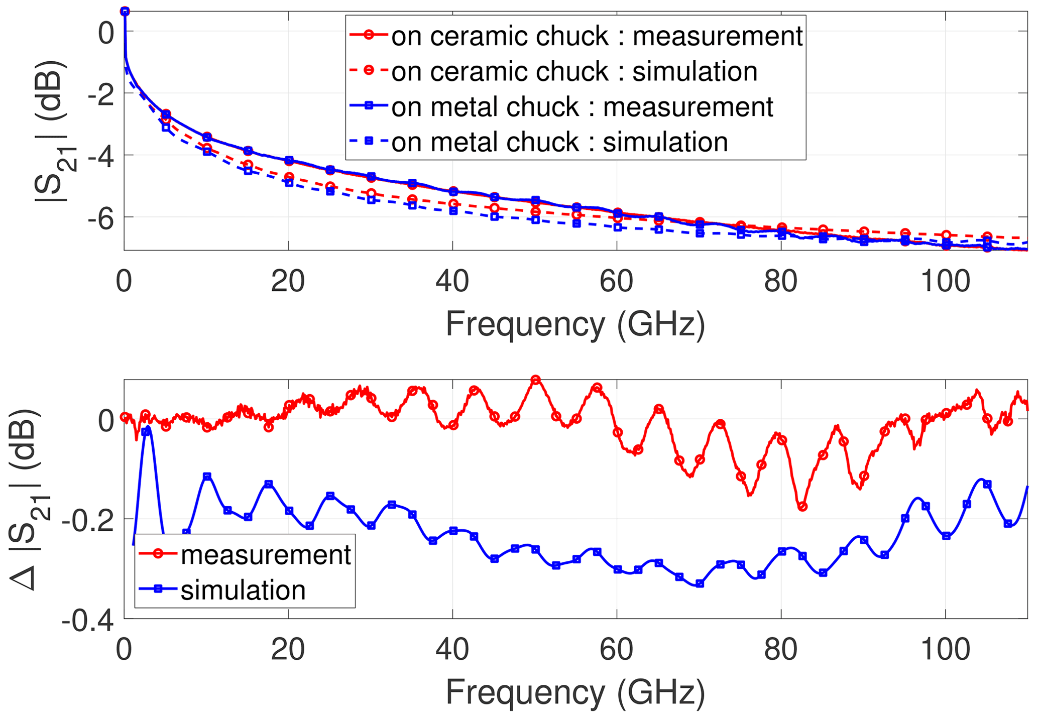
Figure 1Measurement and EM simulation of the CPW with l = 11 400 µm on different chuck materials: Magnitude of transmission coefficient and difference between transmission on metal and ceramic chuck.
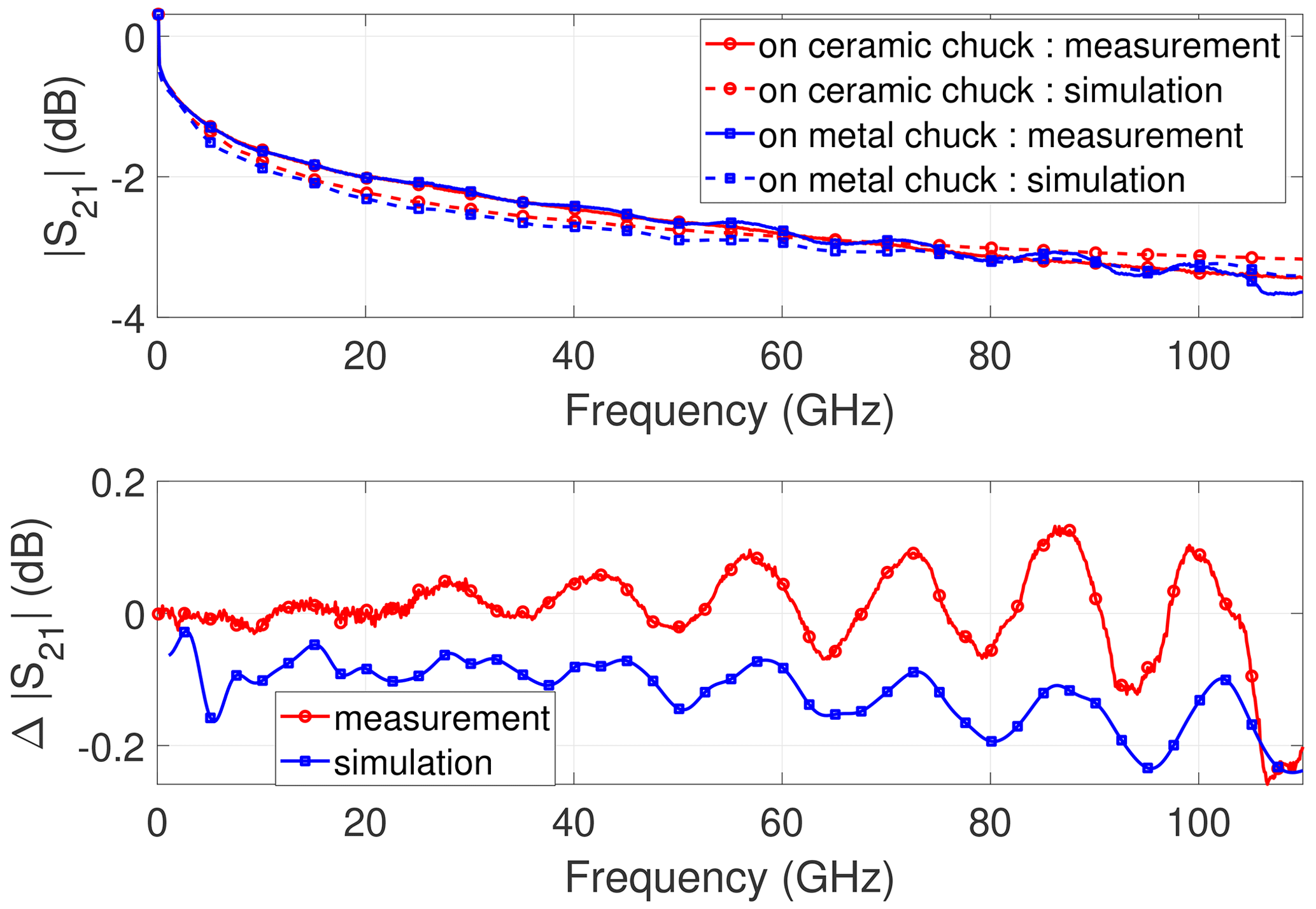
Figure 2Measurement and EM simulation of the CPW with l = 5400 µm on different chuck materials: Magnitude of transmission coefficient and difference between transmission on metal and ceramic chuck.
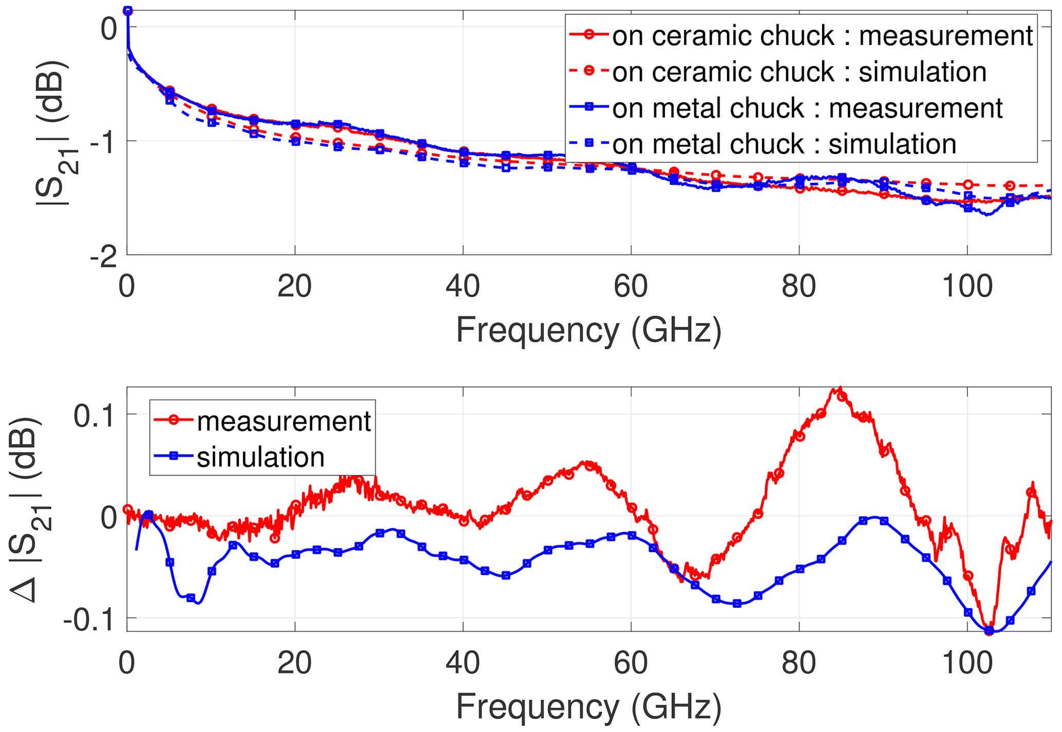
Figure 3Measurement and EM simulation of the CPW with l = 2400 µm on different chuck materials: Magnitude of transmission coefficient and difference between transmission on metal and ceramic chuck.
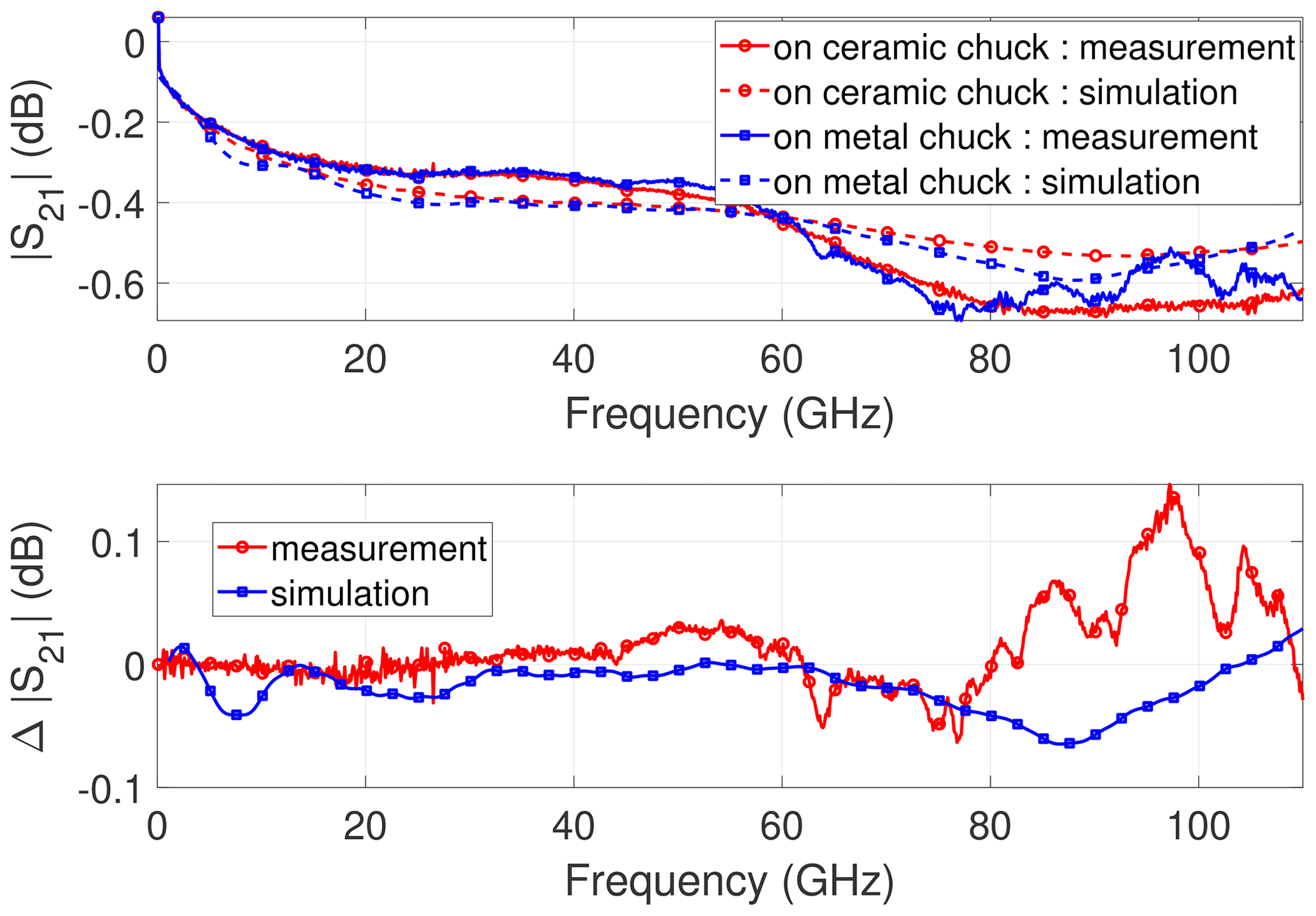
Figure 4Measurement and EM simulation of the CPW with l = 900 µm on different chuck materials: Magnitude of transmission coefficient and difference between transmission on metal and ceramic chuck.
At first sight, one can observe a relatively good agreement between the EM simulation and measurement for all the data. Overall, there is a slight shift between measurements and EM simulation due to not fully known material properties and lack of knowledge of the exact probe geometry (because the manufacturer data of the probes are not available).
When comparing the metal and ceramic chuck, an interesting behavior can be observed: The metal chuck case shows strong ripples in , while the ceramic chuck case shows an ideal smooth curve within the investigated frequency range especially for the longer CPWs. Figure 1 shows the results for the CPW with l = 11 400 µm. Ripples are not only pronounced in but also in the difference calculated according to Eq. (1) with the ceramic chuck as reference. Obviously, the differences of both simulations and measurements show a similar behavior. The ripples are also visible when the CPW length is decreased to l = 5400 µm (Fig. 2) and l = 2400 µm (Fig. 3), respectively. Here, the same statement holds. The metal chuck represents the worst case with strong ripples and the CPWs on ceramic chuck reveal the expected smooth behavior. The periodicity of the ripples also changes when the CPW length is decreased. This behavior can be detected for both measured and simulated data.
The situation changes when comparing the curves corresponding to the CPW with l = 900 µm (Fig. 4). Here, the CPW on the ceramic chuck shows a dip behavior instead of the expected smooth curve behavior. Thus, the ceramic chuck does not represent the ideal case with least parasitics. The peculiarity of the dip behavior can be attributed to the probe-to-probe coupling in too short CPWs (Phung and Arz, 2021a). The mTRL calibration cannot fully eliminate the influence of the probes when the CPW length is below 2 mm. Therefore, the ripple behavior occuring in longer CPWs is different from that of shorter CPWs (e.g. l = 900 µm).
Field plots
So far, the CPW measurements and EM simulations demonstrate ripples for the metal chuck case and a smooth curve behavior for the ceramic chuck. One would assume that this ripple behavior in CB-CPWs is related to the propagation of the PPL mode. In this section, the underlying reasons will be investigated by means of thorough field analysis.
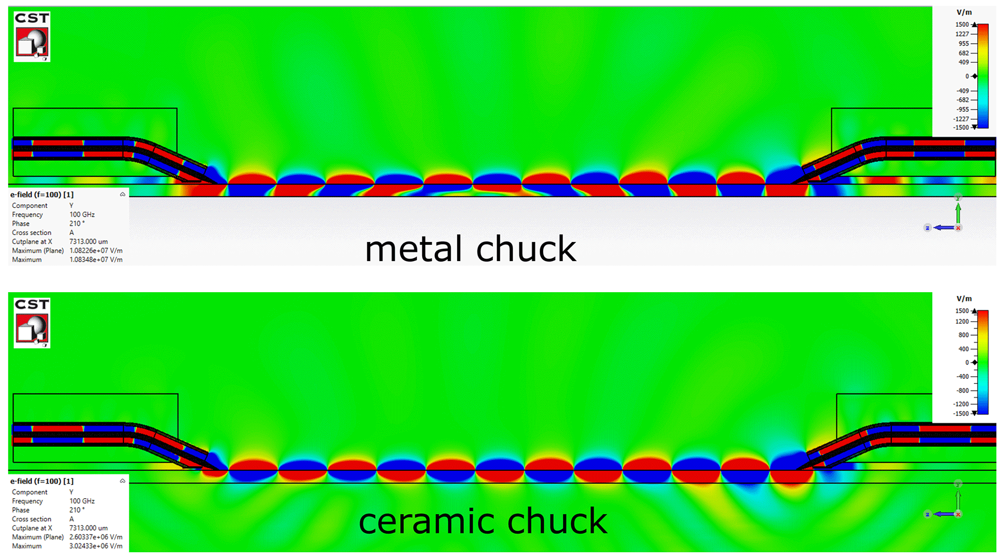
Figure 5Cross-sectional view: simulated vertical electric field component of the CPW with l = 11 400 µm on different chucks at f = 100 GHz.
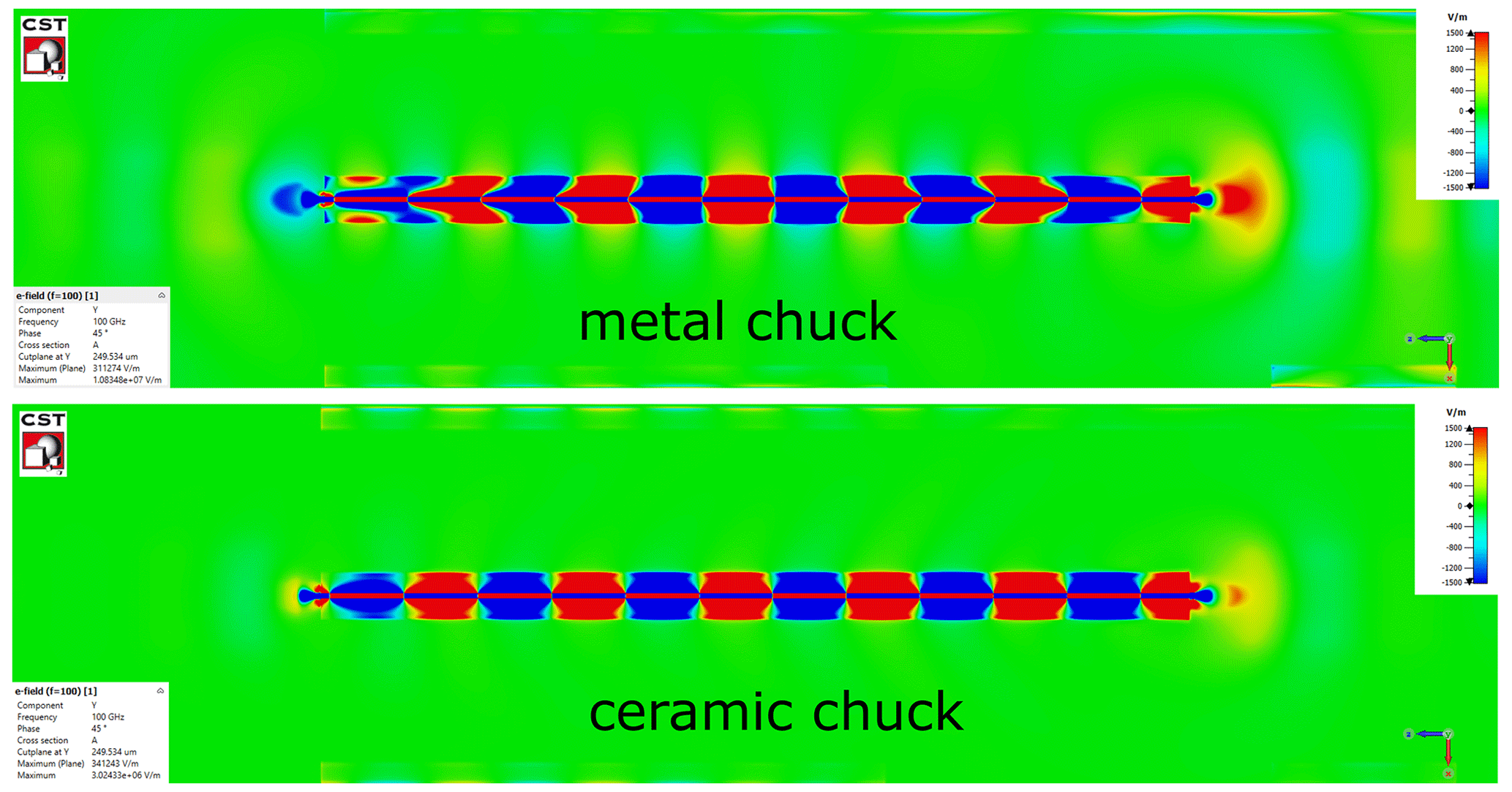
Figure 6Top view: simulated vertical electric field component of the CPW with l = 11 400 µm on different chucks at f = 100 GHz.
Figures 5 and 6 show the cross-sectional and top view of the EM simulated vertical electric field component for the longest CPW with l = 11 400 µm. The scaling of the vertical electric field is exaggerated in order to clarify the pronounced effects. When comparing the vertical electric field component of the CPW placed on the ceramic chuck against that on the metal chuck at cross-sectional view (Fig. 5), one can clearly detect an undisturbed CPW mode propagation for the ceramic chuck. The field plots for the metal chuck show the propagation and superposition of two modes. The CPW mode on the ceramic chuck propagates with a constant phase velocity, whereas on the metal chuck, two modes, the CPW and the PPL mode, are propagating with two different phase velocities. The divergent phase velocities can be traced back to different effective permittivities. The PPL mode has a larger phase constant βPPL>βCPW, thus leakage behavior is unavoidable.
Additionally, one can observe that the PPL mode is not only propagating along the CPW line, but is also supported by the probe needles and transferred into the air region surrounded by the absorber enclosing the coaxial line of the probe and the calibration substrate. The superposition of the CPW with the PPL mode leads to constructive and destructive interference of the electric fields which result in phase distortions along the CPW (see Fig. 5).
The fields in the top view of Fig. 6 also confirm this statement. For the ceramic chuck the electric fields of the CPW are mainly concentrated in the gap region and show a regular field pattern. Therefore, whenever the vertical electric field component at the signal conductor reaches its maximum field strength (red), the vertical electric field component at the two CPW ground reaches the minimum field strength (blue) and vice versa. This consistent field pattern is a clear evidence of a pure CPW mode propagation.
The metal chuck, however, reveals a different electric field pattern. The total CPW width (which is two times the CPW ground width plus the spacing) forms the upper metal plate and the backside the bottom plate guiding the PPL mode. The field of the PPL mode is concentrated inside the substrate supported by the two metal plates. Thus, its expected field pattern is characterized by vertical electric field components which are oriented perpendicularly to the CPW surface. The vertical electric field component on the upper plate (CPW total width) either reaches its maximum (red) or its minimum (blue). The superposition of the CPW mode and the PPL mode distorts the field pattern (see metal chuck case in Fig. 6).
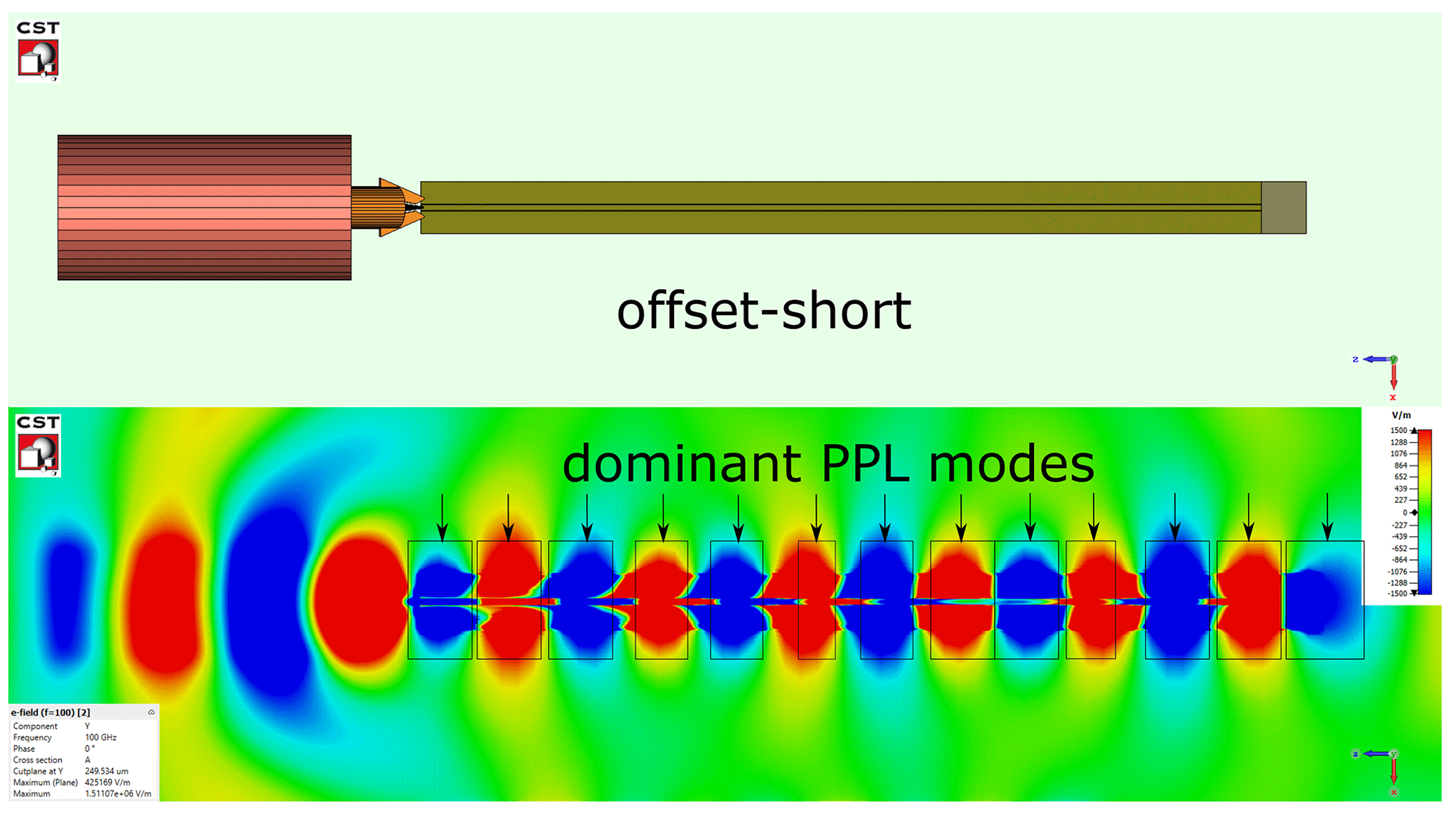
Figure 7Top view: simulated vertical electric field component of an offset short on metal chuck.
In order to demonstrate the effect of the PPL mode more clearly, an offset short is simulated for comparison (Fig. 7). Here, the vertical electric field component is undoubtedly perpendicular to the CPW surface. The electric field reaches its maximum or reaches its minimum on the upper plate (enclosing the CPW total width). Therefore, the expected propagation of the PPL mode can be confirmed.
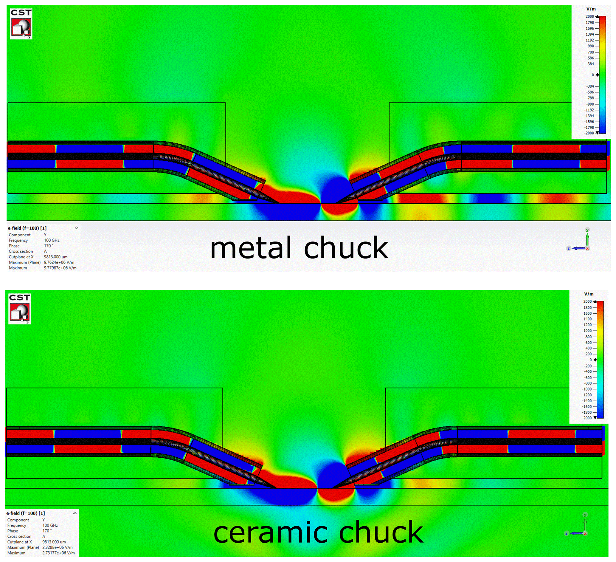
Figure 8Cross-sectional view: simulated vertical electric field component of the CPW with l = 900 µm on different chucks.
So far, the propagation of the PPL mode has been investigated for longer CB-CPWs. This behavior is also evident in the field plots of the CPW with shorter line length l = 900 µm (Fig. 8). Here, due to the shorter CPW length the parasitic probe effects become more evident in both cases, metal and ceramic chuck. For the metal chuck, a strong interaction of the PPL mode with the parasitic probe effects can be observed. The PPL mode is transferred to the regions around the probe needles, the transition to coaxial extensions and between the absorber of probe and calibration substrate. The ripples occuring in the measurements are not only related to the propagation of the PPL mode, but also to the probe properties. To confirm this observation, in the following, a systematic study is performed by varying the probe dimensions.
The first step of the systematic study is to simplify the configuration by using one single CPW excited by the probes. Thus, the interference of neighboring structures is not included in the simulations. Additionally, in order to focus on probe influences, lossless materials are used for both the calibration substrate and the ceramic chuck, i.e. the dielectric loss tangent is set to zero. As can be detected from the field plots (Fig. 5), the probe needle length strongly affects the propagation path of the PPL mode. The probe angle under which the probe touches down influences the strength of the electric fields. Therefore, in this study the parameters under investigation are the probe needle length ln, and the probe angle α (Fig. 9).
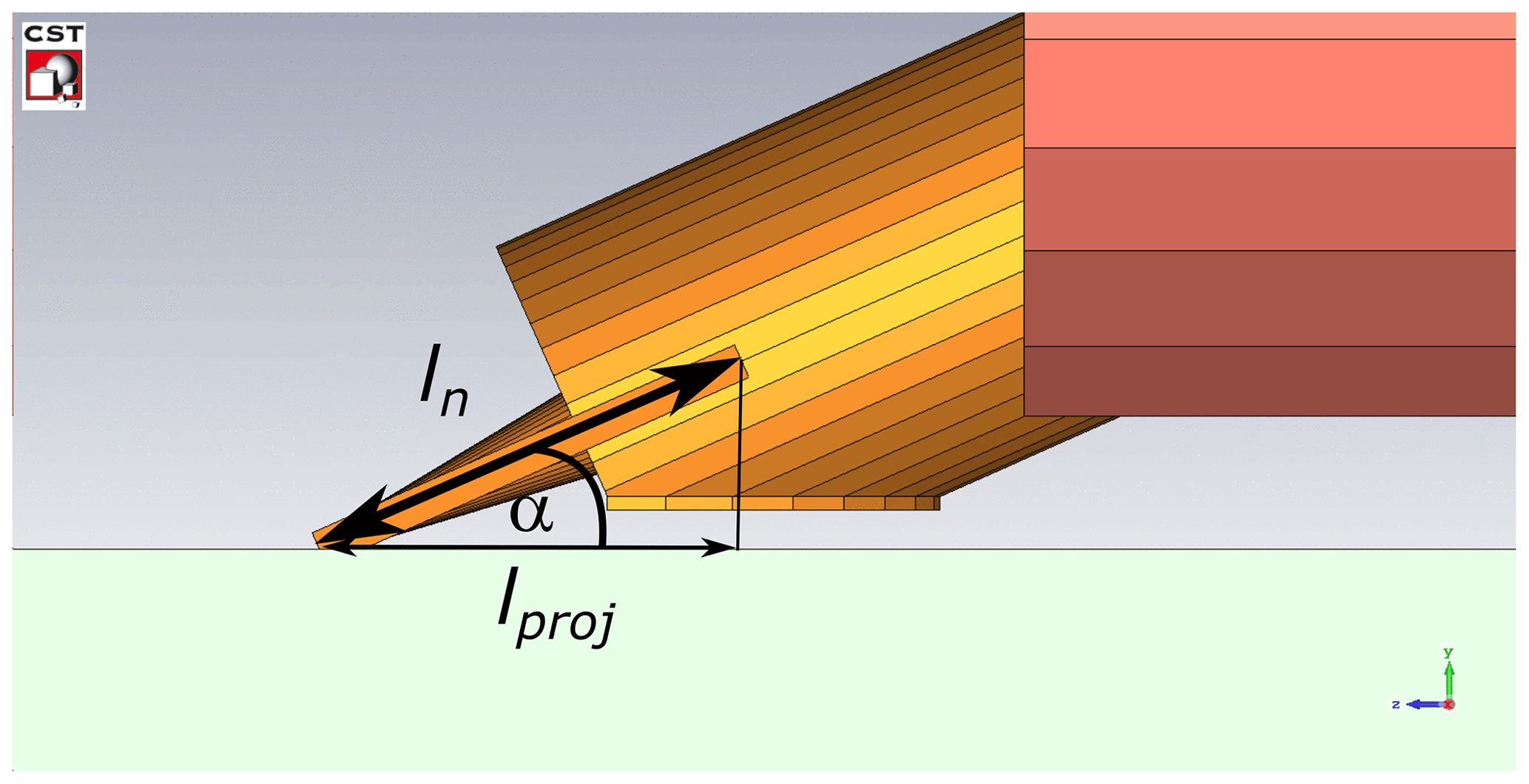
The probe needle length is varied between ln = 150, 320 and 600 µm and the probe angle α is varied between α = 30 and 40∘.
3.1 Influence of probe needle length
Figures 10 and 11 show the simulated and mTRL-calibrated transmission coefficient magnitude of the single CPWs with lengths l = 11 400 µm and l = 900 µm, respectively excited by probes with varied needle lengths under different chuck conditions. The results demonstrate that the probe needle length has a strong impact on the calibrated results for both line lengths. For l = 900 µm, the curve behavior of and the shape of the dip behavior in show a strong dependency on the probe needle length for both chucks. The needle length changes the frequencies of the local minima in as well as in . For the ceramic chuck a strong wavy curve behavior of can be observed. The wavy curve behavior is caused by mTRL calibration artifacts as explained in Phung and Arz (2021a). Thus, the relative difference plot of does not represent a reliable figure of merit.
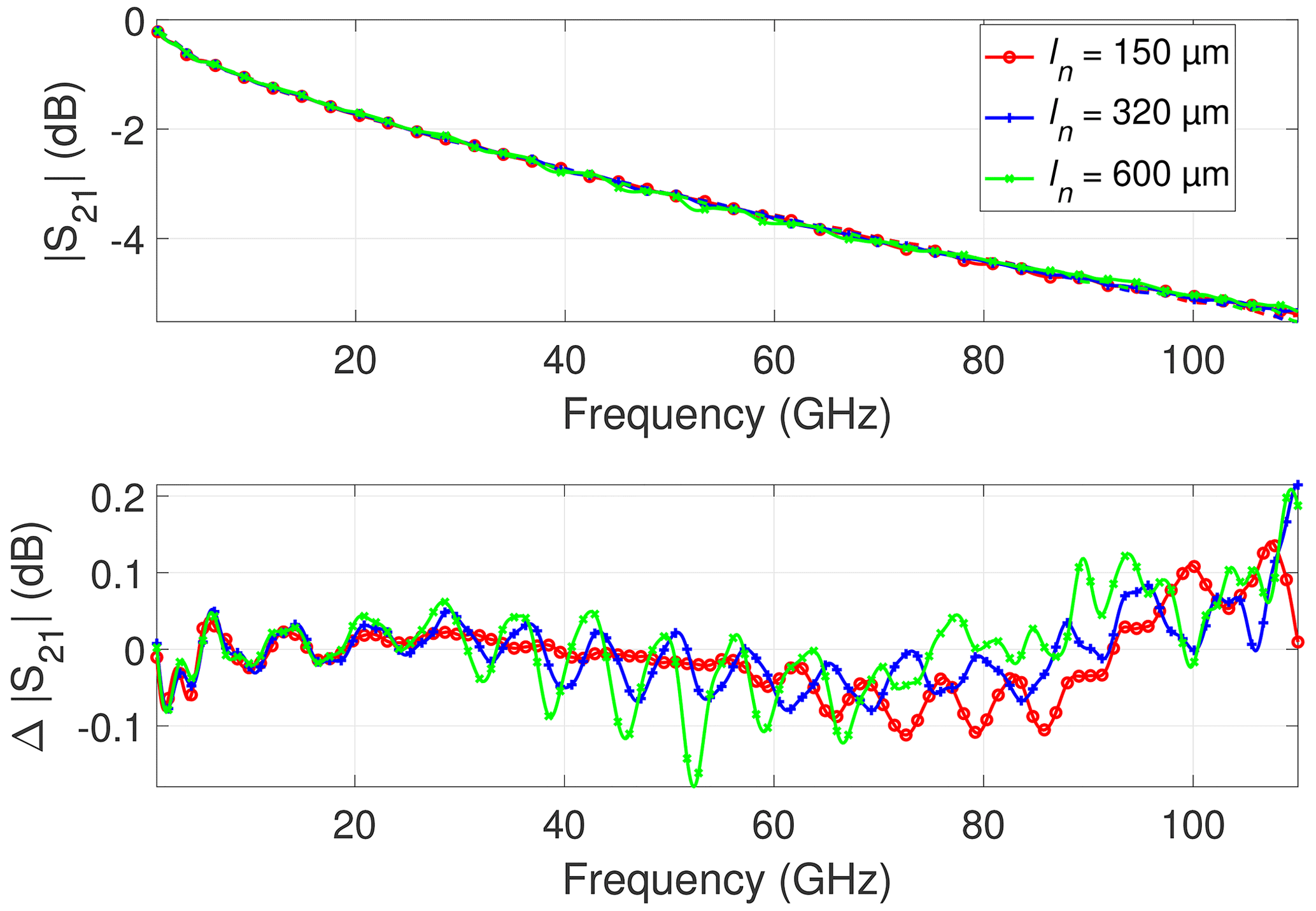
Figure 10Influence of probe needle length ln for the CPW with l = 11 400 µm on different chuck materials: Simulated transmission coefficient magnitude (solid line: on metal chuck; dashed line: on ceramic chuck) and difference between transmission on metal and ceramic chuck.
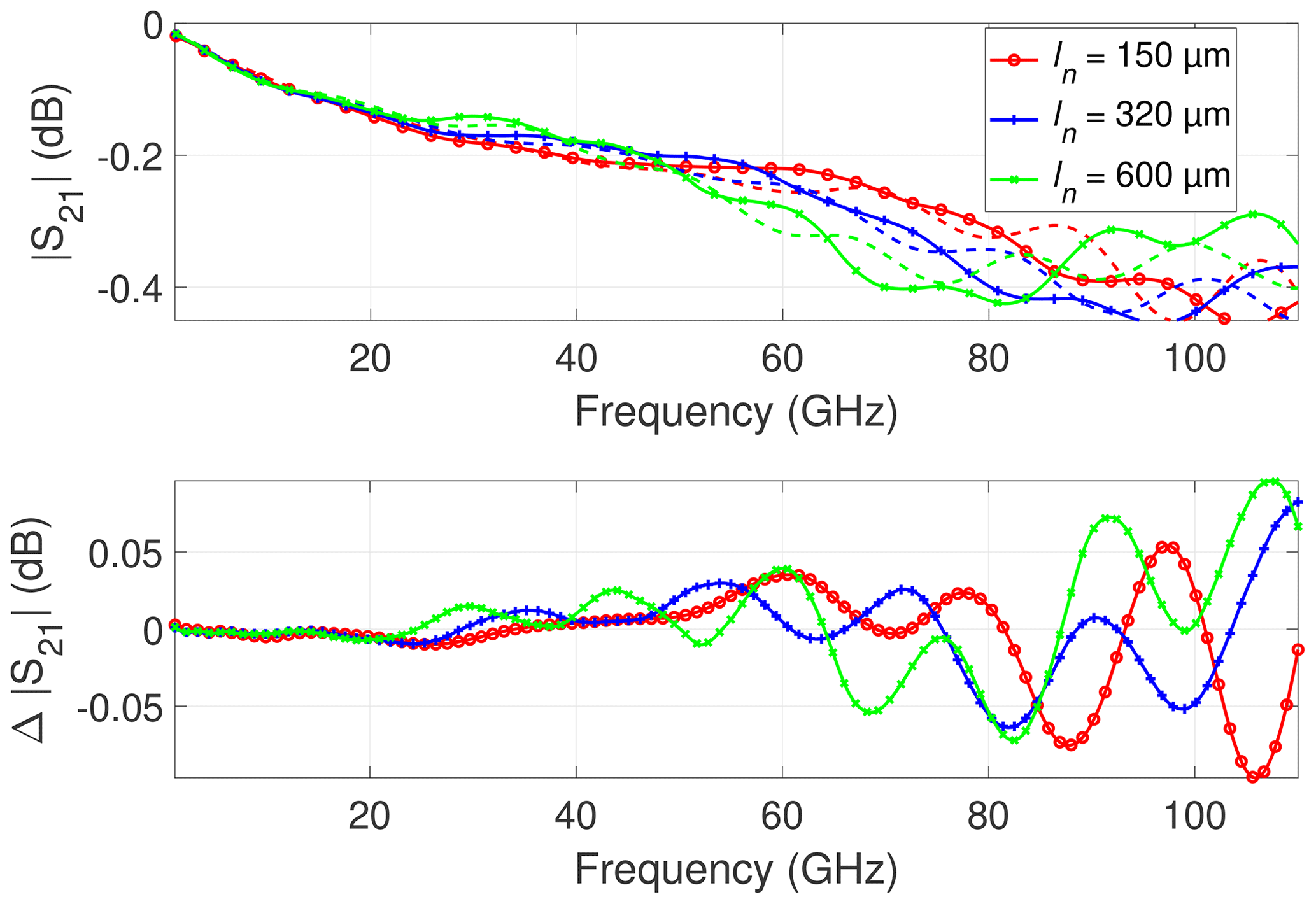
Figure 11Influence of probe needle length ln for the CPW with l = 900 µm on different chuck materials: Simulated transmission coefficient magnitude (solid line: on metal chuck; dashed line: on ceramic chuck) and difference between transmission on metal and ceramic chuck.
For longer CPWs, the situation changes. The ceramic chuck represents the ideal case as shown in Fig. 10. The needle length also has a tremendous impact on the resulting calibrated transmission coefficient S21. The ripples are more pronounced particularly for the longer probe needle length ln = 600 µm. The distance between the ripples decreases with increasing probe needle length. This can be observed in of Fig. 10 and clearly proves that the probe needle length is an essential part of the propagation path of the PPL mode.
3.2 Influence of probe angle
So far, it has been found that the probe needle length has a clear impact on the occurrence of the ripples over frequency. The next question is how the ripples change with the probe angle. Figure 12 shows the results for the CPW with l = 11 400 µm when varying the probe angle. From Fig. 12 it can be concluded that the probe angle only has a rather minor influence on the values of and .
Figure 12Influence of probe angle α for the CPW with l = 11 400 µm on different chucks: Transmission coefficient magnitude (solid line: on metal chuck; dashed line: on ceramic chuck) and difference between transmission on metal and ceramic chuck.
The systematic study in the previous section clearly shows that the resonance effects or ripples are related to the PPL mode and parasitic probe effects. The probe needle length determines the frequencies where the resonances occur. Therefore, an analytical model to qualitatively predict the resonance effects is developed. The first step of the analytical approach is to extract the resonant frequencies for the different CPW lengths based on from EM simulation and measurement.
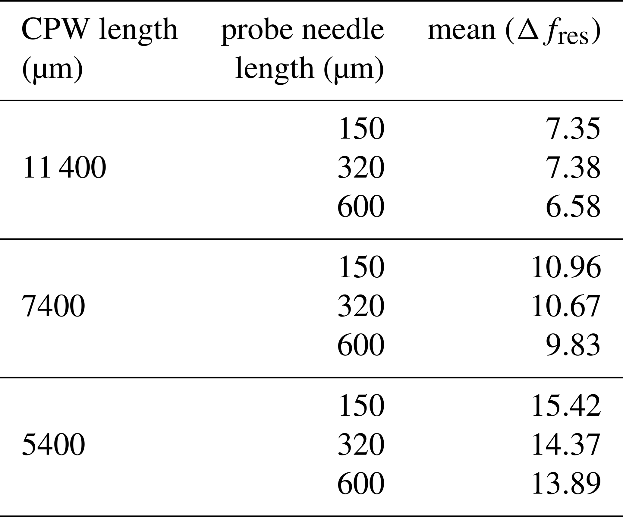
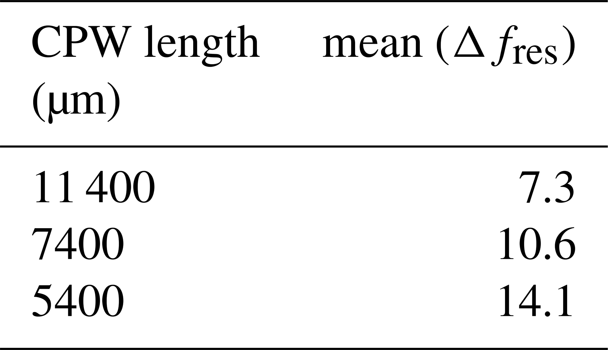
Figure 13 shows the extraction procedure for the simulated and measured data using according to Eq. (1). Table 1 shows the mean of the differences between the extracted resonant frequencies Δfres based on the simulated data for different probe needle lengths and CPW lengths. Table 2 presents the corresponding data for the measured results with varied CPW lengths. Comparing the results of Tables 1 and 2, it can be seen that the measured resonant frequencies for different CPW lengths coincide well with the simulated resonant frequencies for a probe needle length of ln = 320 µm. This good agreement indicates that the simulated probe model sufficiently reproduces the probe used in real measurements.
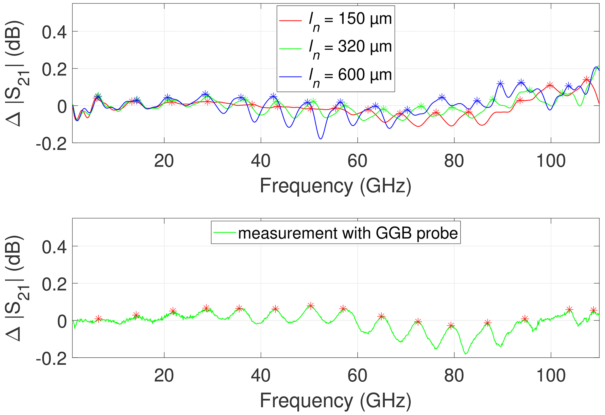
Figure 13Extraction of resonant frequencies from simulation for different probe needle lengths ln and from measurement with GGB probe: Differences between transmission on metal and ceramic chuck.
Table 1Mean resonant frequencies extracted from EM simulation.
The next section presents an analytical description to predict the occurence of the resonant effects depending on the probe needle length and probe angle.
The analytical description of the resonant frequency is found based on the results of the extraction procedure (Fig. 13). In this description, it is important to include all parameters that determine the propagation path of the PPL mode.
Figure 14 illustrates the relevant parameters which are the CPW length l, the line extension ΔlH according to Hammerstad (1975), and the probe length projection lproj.
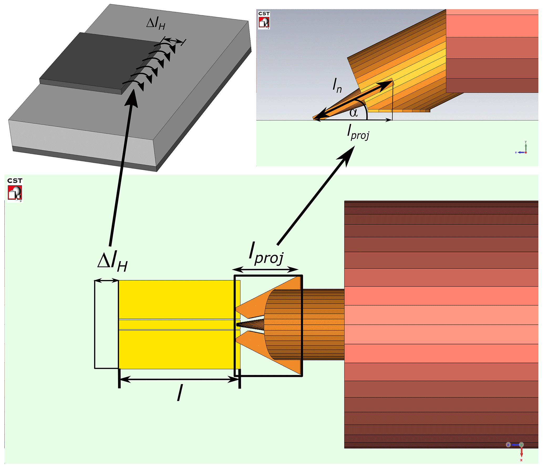
l represents the total CPW length and describes the propagation path of the PPL mode along the CPW line.
ΔlH in Eq. (2) describes the stray fields of the PPL mode at the end of the CPW line, which cause an effective length extension (Hammerstad, 1975). The total CPW width forms the upper plate of the PPL mode which is mainly concentrated inside the calibration substrate. Therefore, the total CPW width wtot (Eq. 3), the substrate thickness h and the effective permittivity ϵreff,PPL are accounted for in the effective length extension (Eq. 2). The effective permittivity ϵreff,PPL of the PPL or microstrip mode is calculated by the analytical description of the microstrip model of Schnieder and Heinrich (2001).
lproj in Eq. (4) describes the projection (shadow) of the probe needle length (see also Fig. 9) for the propagation path of the PPL mode which travels to the probe needles (see Fig. 8).
The resonant frequencies are associated with half-wave length resonances. The difference between resonant frequencies determining the frequency occurrence of the ripples can be calculated by the two alternative Eqs. (5) and (6):
Equation (5) describes the resonant frequency behavior including the effect of the CPW length l, the effective length extension ΔlH of Hammerstad (1975), and the effective permittivity ϵreff,PPL according to Schnieder and Heinrich (2001). Equation (6) additionally takes into account the effect of the probe needle projection using the probe needle length ln and the probe angle α.
To validate the proposed analytical descriptions, results calculated from Eqs. (5) and (6) are presented in the following. Figure 15 presents the calculations of Eqs. (5) and (6) in comparison with the results extracted from measurements for the different CPW lengths l, as given in Table 2. Obviously, the resonant frequencies extracted from measurements show a better agreement with the resonant frequencies calculated from Eq. (6) in comparison to Eq. (5). This proves that the probe needle length has a large impact on the ripples and needs to be accounted for. Thus, Eq. (6) represents a good model equation for the occurrence of the ripples observed.
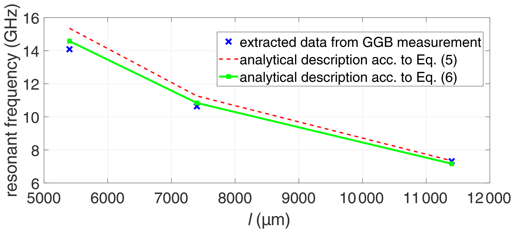
Figure 15Extraction of resonant frequencies for measured data of the CPW on SiO2 substrate: resonant frequency vs. line length l.
Due to the limited number of CPWs on fused silica substrate, the number of available CPW measurements was rather small. Therefore, simulations of CPWs with additional line lengths were performed to further verify Eq. (6). The extraction procedure was repeated for the additional simulated data with a probe needle length of ln = 320 µm.
Figure 16 shows the comparison of the calculations according to Eqs. (5) and (6) together with the results from the simulations. Here again, the calculated data according to Eq. (5) without the influence of probe needle shows worse agreement with the EM simulated extracted data, while Eq. (6), on the other hand, shows excellent agreement.
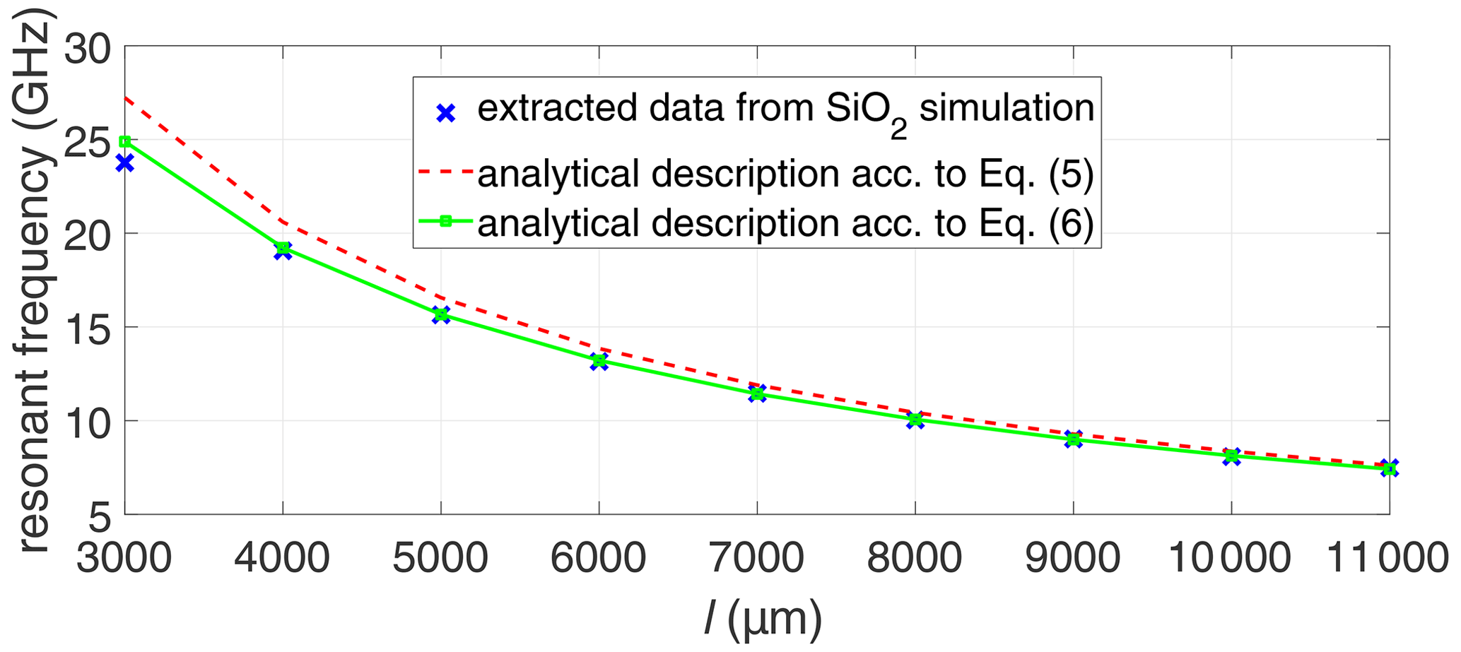
Figure 16Extraction of resonant frequencies for simulated data of the CPW on SiO2 substrate: resonant frequency vs. line length l.
Verification of analytical description on Al2O3 substrate
So far, results for CPWs manufactured on a fused silica substrate have been presented, and the validity of the newly developed analytical description Eq. (6) has been verified for this material with ϵr = 3.78. The next question to be addressed is whether Eq. (6) is also valid for other substrate materials. To this end, the measurements on both chuck conditions were repeated for Al2O3 substrate which has also been used in Probst et al. (2017), Phung et al. (2021), and Phung et al. (2018b). The measurements were then corrected via mTRL calibration. The extraction procedure of the resonant frequencies was repeated accordingly. The extracted data were then compared with the predictions from eqs. (5) and (6).
As shown in Fig. 17, no clear conclusion can be drawn. Eq. (5) seems to show better agreement with the measured extracted data for longer CPWs, e.g. l = 7400 µm and l = 11 400 µm. For shorter CPWs, e.g. l = 5400 µm or l = 2400 µm, however, the extracted results of Eq. (6) agree better with the measured extracted data.
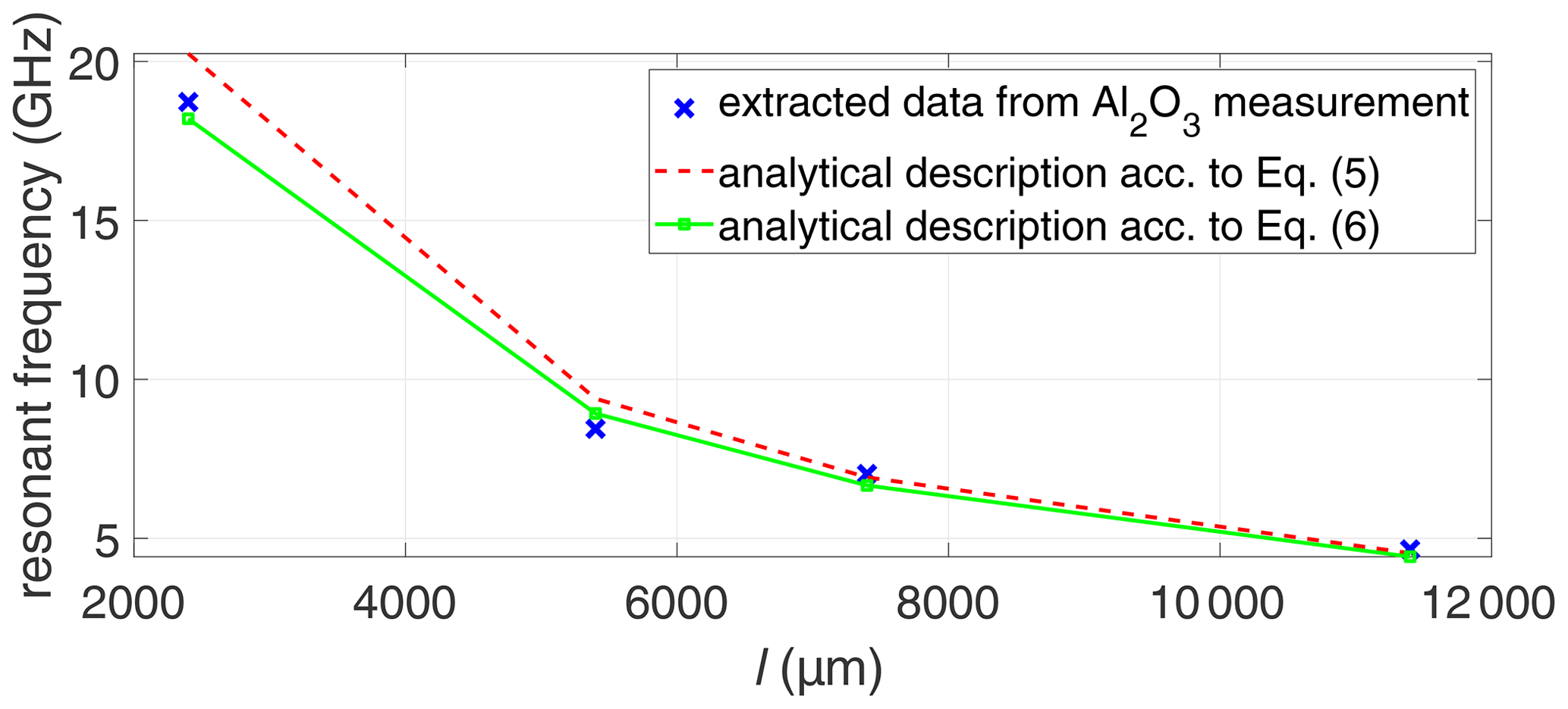
Figure 17Extraction of resonant frequencies from Al2O3 measurements: resonant frequency vs. line length l.
The reason for the observed ambiguities can be found in the extraction procedure of the measured data, which is far from being flawless. Figure 18 plots the extraction of resonant frequencies for Al2O3 measurement for the CPW with l = 11 400 µm. The measured data are too noisy for an automatic extraction which therefore has been performed manually with additional uncertainties compared to an automatic process.
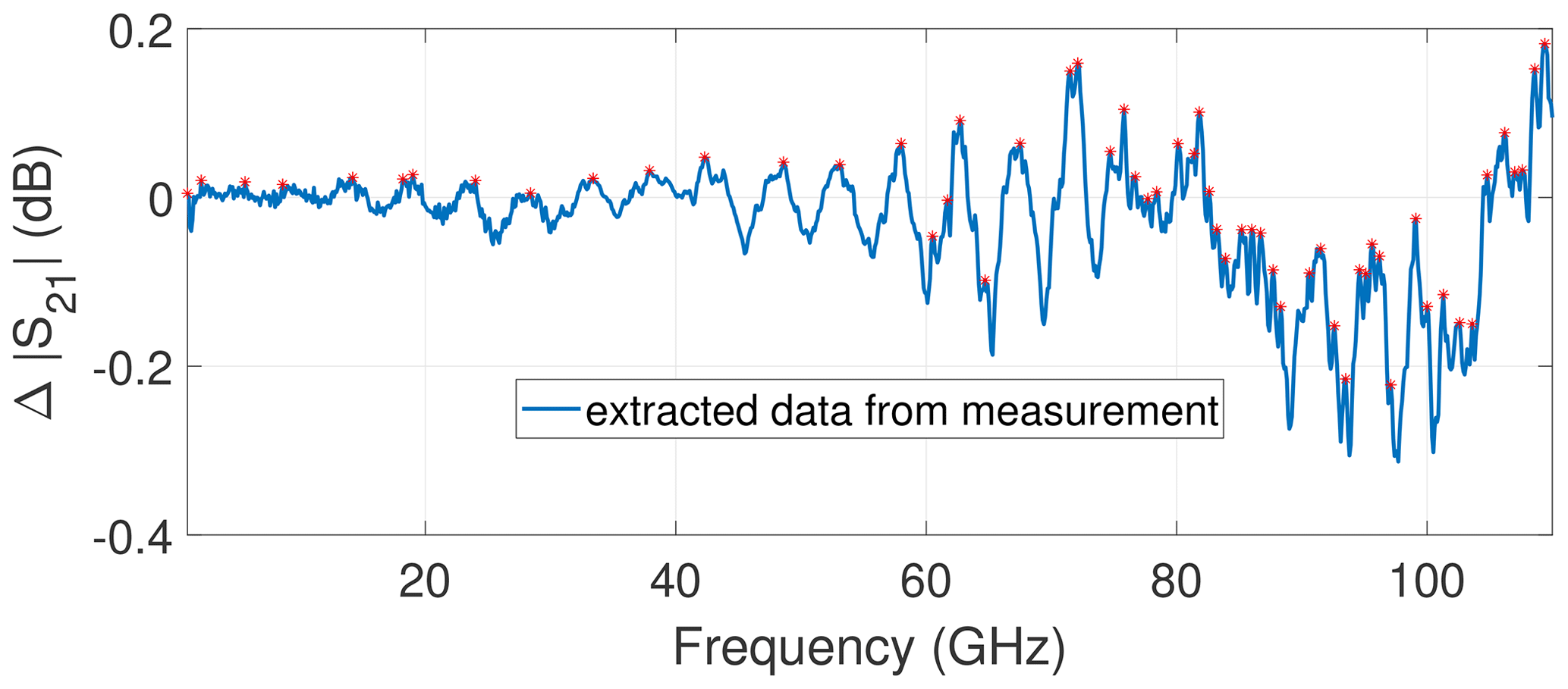
Figure 18Extraction of resonant frequencies from Al2O3 measurements: Difference between transmission on metal and ceramic chuck for the CPW with l = 11 400 µm.
As EM simulation data are expected to be less noisy, the simulation of the complete calibration set and CPWs with additional lengths was repeated, followed by the extraction of the resonant frequencies.
The extracted data are plotted in Fig. 19 and compared with the predictions from Eqs. (5) and (6). From Fig. 19, a clear conclusion is possible: Eq. (6) shows excellent agreement with the simulated extracted data.
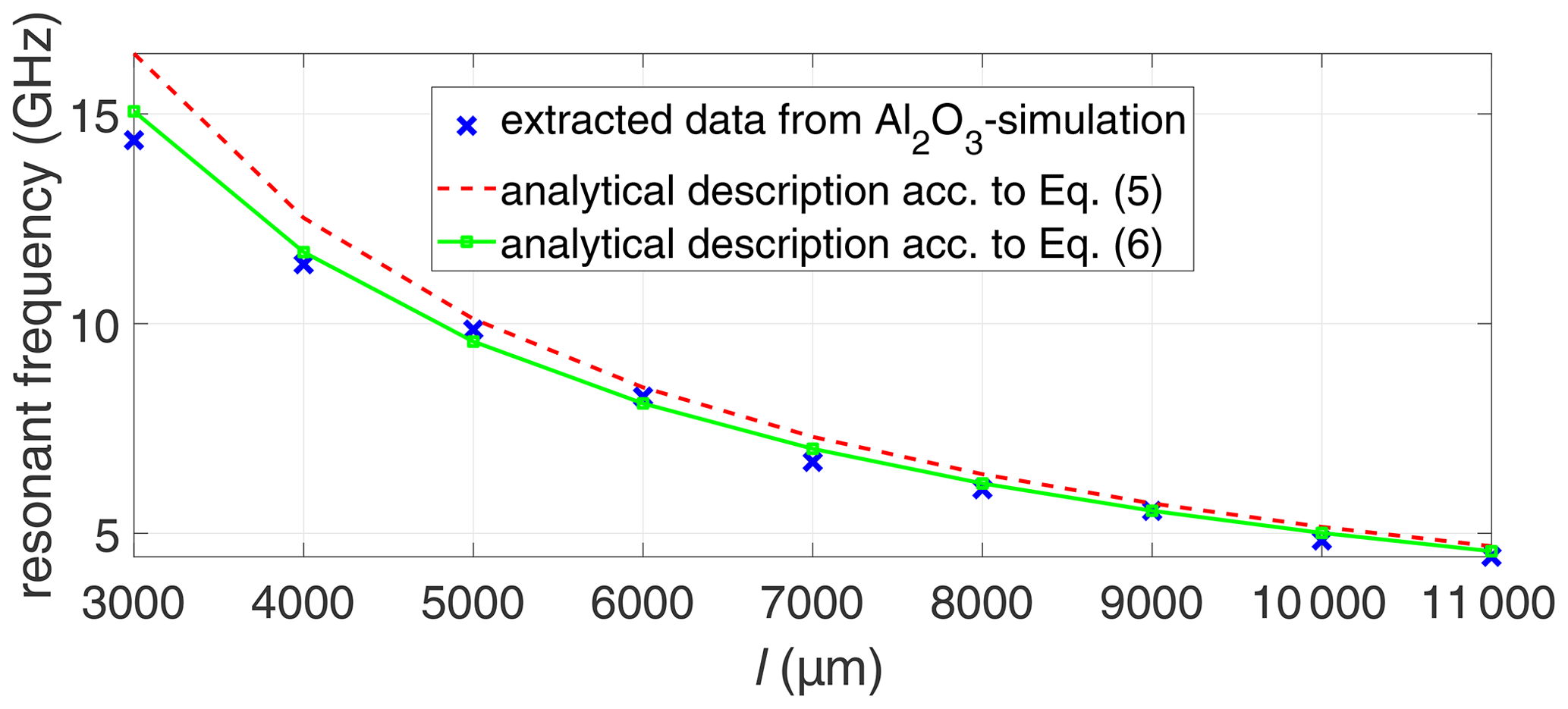
Figure 19Extraction of resonant frequencies for simulated data of the CPW on Al2O3 substrate: resonant frequency vs. line length l.
This proves that the validity of the analytical description can also be confirmed for other materials such as e.g. alumina. Further investigations (not shown here) reveal that Eq. (6) is also valid for other probe types.
Summarizing the above results, this paper demonstrates how probe effects deteriorate mTRL-calibrated S-parameter measurements of CB-CPW structures. This paper does not only present a thorough study of CB-CPWs through field analysis but also proposes an analytical description to predict the occurrence of ripples and resonance effects taking the probe geometries into account. For the first time, an analytical description of PPL resonances in combination with parasitic probe effects is presented. The analytical description is verified by EM simulation and measurement for two different substrate materials, i.e. fused silica and alumina.
No software code or research data is available for the presented work, but all results can be reproduced with the equations and parameters given here.
GNP has performed the electromagnetic simulations. UA has devised the main conceptual ideas. Based on the analysis of the measured and simulated results, they have developed the analytical formula.
The contact author has declared that neither of the authors has any competing interests.
Publisher’s note: Copernicus Publications remains neutral with regard to jurisdictional claims in published maps and institutional affiliations.
This article is part of the special issue “Kleinheubacher Berichte 2021”.
The authors acknowledge support by the European Metrology Programme for Innovation and Research (EMPIR) Project 14IND02 “Microwave measurements for planar circuits and components”. Furthermore, this work was supported in part by the Project 20IND03 FutureCom “RF Measurements for future communications applications”. Both projects (14IND02 and 20IND03) have received funding from the EMPIR programme co-financed by the Participating States and from the European Union's Horizon 2020 research and innovation programme.
The authors are also grateful to Rohde & Schwarz for manufacturing the calibration substrates used in this study. The authors also thank Dirk Schubert from PTB for his expert technical assistance.
This research has been supported by the European Association of National Metrology Institutes (grant nos. EMPIR 14IND02 PlanarCal and EMPIR 20IND03 FutureCom).
This paper was edited by Thorsten Schrader and reviewed by two anonymous referees.
Amado-Rey, B., Tessmann, A., Campos-Roca, Y., Massler, H., Leuther, A., and Ambacher, O.: Spurious Mode Suppression in the Design of GCPW Submillimeter-wave Power Amplifiers, in: 2018 48th European Microwave Conference (EuMC), 23–27 September 2018, Madrid, Spain, IEEE, 851–854, https://doi.org/10.23919/EuMC.2018.8541553, 2018. a
Arz, U., Kuhlmann, K., Dziomba, T., Hechtfischer, G., Phung, G. N., Schmückle, F. J., and Heinrich, W.: Traceable Coplanar Waveguide Calibrations on Fused Silica Substrates up to 110 GHz, IEEE T. Microw. Theory, 67, 2423–2432, 2019. a, b
CST Studio Suite: https://www.3ds.com/products-services/simulia/products/cst-studio-suite/ (last access: 25 April 2023), 2020. a, b
EMPIR: Microwave Measurements for Planar Circuits and Components, European Metrology Programme for Innovation and Research JRP Number 14IND02, https://planarcal.ptb.de, last access: 25 April 2023. a
Fregonese, S., De matos, M., Deng, M., Potereau, M., Ayela, C., Aufinger, K., and Zimmer, T.: On-Wafer Characterization of Silicon Transistors Up To 500 GHz and Analysis of Measurement Discontinuities Between the Frequency Bands, IEEE T. Microw. Theory, 66, 3332–3341, 2018. a
Godshalk, E. M.: Surface Wave Phenomenon in Wafer Probing Environments, in: 40th ARFTG Conference Digest, 3–4 December 1992, Orlando, FL, USA, IEEE, vol. 22, 10–19, https://doi.org/10.1109/ARFTG.1992.326994, 1992. a
Hammerstad, E. O.: Equations for Microstrip Circuit Design, in: 1975 5th European Microwave Conference, 1–4 September 1975, Hamburg, Germany, IEEE, 268–272, https://doi.org/10.1109/EUMA.1975.332206, 1975. a, b, c
Lee, G.-A. and Lee, H.-Y.: Suppression of the CPW Leakage in Common Millimeter-Wave Flip-Chip Structures, IEEE Microw. Guided W., 8, 366–368, https://doi.org/10.1109/75.736245, 1998. a
Liu, Y. and Itoh, T.: Leakage Phenomena in Multilayered Conductor-Backed Coplanar Waveguides, IEEE Microw. Guided W., 3, 426–427, https://doi.org/10.1109/75.248521, 1993. a
Marks, R. B.: A Multiline Method of Network Analyzer Calibration, IEEE T. Microw. Theory, 39, 1205–1215, 1991. a
McKinzie, W. E. and Alexopoulos, N. G.: Leakage Losses for the Dominant Mode of Conductor-Backed Coplanar Waveguide, IEEE Microw. Guided W., 2, 65–66, https://doi.org/10.1109/75.122412, 1992. a
Phung, G. N. and Arz, U.: Anomalies in Multiline-TRL-Corrected Measurements of Short CPW Lines, in: 96th ARFTG Microwave Measurement Symposium (ARFTG), 18–22 January 2021, San Diego, CA, USA, IEEE, 1–4, https://doi.org/10.1109/ARFTG49670.2021.9425345, 2021a. a, b
Phung, G. N. and Arz, U.: Parasitic Probe Effects in Measurements of Conductor-Backed Coplanar Waveguides, in: 2021 Kleinheubach Conference, 28–30 September 2021, Miltengerg, Germany, IEEE, 1–4, https://doi.org/10.23919/IEEECONF54431.2021.9598396, 2021b. a
Phung, G. N., Schmückle, F. J., Doerner, R., Heinrich, W., Probst, T., and Arz, U.: Impact of Substrate Modes on mTRL-Calibrated CPW Measurements in G Band, in: 2018 48th European Microwave Conference (EuMC), 23–27 September 2018, Madrid, Spain, IEEE, 194–197, https://doi.org/10.23919/EuMC.2018.8541813, 2018a. a
Phung, G. N., Schmückle, F. J., Doerner, R., Heinrich, W., Probst, T., and Arz, U.: Effects Degrading Accuracy of CPW mTRL Calibration at W Band, in: 2018 IEEE/MTT-S International Microwave Symposium – IMS, 10–15 June 2018, Philadelphia, PA, USA, IEEE, 1296–1299, https://doi.org/10.1109/MWSYM.2018.8439837, 2018b. a, b
Phung, G. N., Schmückle, F. J., Doerner, R., Kähne, B., Fritzsch, T., Arz, U., and Heinrich, W.: Influence of Microwave Probes on Calibrated On-Wafer Measurements, IEEE T. Microw. Theory, 67, 1892–1900, https://doi.org/10.1109/TMTT.2019.2903400, 2019. a, b
Phung, G. N., Arz, U., Kuhlmann, K., Doerner, R., and Heinrich, W.: Improved Modeling of Radiation Effects in Coplanar Waveguides with Finite Ground Width, in: 2020 50th European Microwave Conference (EuMC), 12–14 January 2021, Utrecht, the Netherlands, IEEE, 404–407, https://doi.org/10.23919/EuMC48046.2021.9338133, 2021. a
Probst, T., Doerner, R., Ohlrogge, M., Lozar, R., and Arz, U.: 110 GHz On-Wafer Measurement Comparison on Alumina Substrate, in: 2017 90th ARFTG Microwave Measurement Symposium (ARFTG), 28 November–1 December 2017, Boulder, CO, USA, IEEE, 1–4, https://doi.org/10.1109/ARFTG.2017.8255867, 2017. a
Schnieder, F. and Heinrich, W.: Model of Thin-Film Microstrip Line for Circuit Design, IEEE T. Microw. Theory, 49, 104–110, https://doi.org/10.1109/22.899967, 2001. a, b
Shigesawa, H., Tsuji, M., and Oliner, A. A.: A New Mode-Coupling Effect on Coplanar Waveguides of Finite Width, in: IEEE International Digest on Microwave Symposium, 8–10 May 1990, Dallas, TX, USA, IEEE, vol. 3, 1063–1066, https://doi.org/10.1109/MWSYM.1990.99763, 1990. a
Spirito, M., Arz, U., Phung, G. N., Schmückle, F. J., Heinrich, W., and Lozar, R.: Guidelines for the Design of Calibration Substrates, including the Suppression of Parasitic Modes for Frequencies up to and including 325 GHz, EMPIR 14IND02 – PlanarCal, 2018, Physikalisch-Technische Bundesanstalt (PTB), https://doi.org/10.7795/530.20190424A, 2018a. a, b
Spirito, M., De Martino, C., and Galatro, L.: On the Impact of Radiation Losses in TRL Calibrations, in: 2018 91st ARFTG Microwave Measurement Conference (ARFTG), 15 June 2018, Philadelphia, PA, USA, IEEE, 1–3, https://doi.org/10.1109/ARFTG.2018.8423820, 2018b. a
Tsuji, M., Shigesawa, H., and Oliner, A. A.: New Surface-Wave-Like Mode on CPWs of Infinite Width and its Role in Explaining the Leakage Cancellation Effect, in: 1992 IEEE MTT-S Microwave Symposium Digest, 1–5 June 1992, Albuquerque, NM, USA, IEEE, vol. 1, 495–498, https://doi.org/10.1109/MWSYM.1992.188022, 1992. a
Yadav, C., Deng, M., Fregonese, S., Cabbia, M., De Matos, M., Plano, B., and Zimmer, T.: Importance and Requirement of Frequency Band Specific RF Probes EM Models in Sub-THz and THz Measurements up to 500 GHz, IEEE T. Thz. Sci. Techn., 10, 558–563, 2020. a
- Abstract
- Introduction
- Measurement and simulation results
- Systematic study of probe properties
- Extraction of resonant frequencies
- Analytical description for resonant frequencies
- Conclusions
- Code and data availability
- Author contributions
- Competing interests
- Disclaimer
- Special issue statement
- Acknowledgements
- Financial support
- Review statement
- References