 | 20 Aug 2024
Iterative Placement of Decoupling Capacitors using Optimization Algorithms and Machine Learning
Zouhair Nezhi
Nima Ghafarian Shoaee
Marcus Stiemer
In this work, an approach for optimum placement of on-board decoupling capacitors (decaps) is presented, which aims at reducing transient noise in power delivery networks (PDNs). This approach is based on a genetic algorithm (GA) and accelerated by the use of an artificial neural network (ANN) as surrogate model to efficiently determine the fitness of a decap design, i.e., of a particular choice for the position and the type of the decaps to integrate in the printed circuit board (PCB). The ANN is trained by a suitable set of reference designs labeled by the impedance at the power pin of the integrated circuit (IC), which is computed by commercial simulation software. Several iterative runs of the GA are performed with an increasing number of decaps to identify a design with the least number of decaps necessary to reduce the distance of the frequency domain input impedance of the considered point-to-point connection from a desired target impedance as far as possible. This approach is successfully applied to generate an optimum decap design for a PDN with 52 possible decap positions and decaps chosen from three types.
- Article
(1522 KB) - Full-text XML
- BibTeX
- EndNote


Machine Learning (ML) and artificial intelligence (AI) can aid in the layout, component placement, interconnect routing, channel and equalization optimization, and other aspects of PCB design and optimization (Lu et al., 2018). In the design of modern PDN, the placement of decaps is crucial for reducing power supply fluctuations to maintain the functional stability of ICs and to avoid a feedback. To operate reliably, the latter require a high quality DC voltage delivered by the PDN. However, dynamic switching currents induce high frequency currents witch couple into the the PDN and cause transient fluctuations superposing the DC supply of the ICs. The accompanying high-frequency voltage ripples on top of the DC level can negatively impact the ICs operation (e.g., by altering the level of the DC bias the pull-up and pull-down capability of transistors relies on), cause via a feed back to the signal processing on the PCB signal integrity (SI) issues by a feed back to the signal processed on the PCB, and can possibly lead to electromagnetic interference (EMI), because those fluctuations may travel through the PCB and be radiated via antenna like structures, such as, e.g. connectors, slots, or I/O cables (Wu et al., 2010). Consequently, they must be reduced below a certain threshold, which is usually achieved by providing a suitable reserve capacitance, e.g., Swaminathan et al. (2010).
In modern PCB-technology, capacitive decoupling is achieved in various ways depending on the frequencies of the fluctuations. Very high frequencies have to be compensated on the dies via parasitic effects and capacitive coupling between metal layers, e.g., Chuang et al. (2010), Wu et al. (2010). Packages are furnished with on package capacitors (Chen and He, 2007) to handle lower frequencies that are still above 50–100 MHz. Fluctuations at frequencies below 100 MHz are mitigated on the PCB via its plane capacitance or by using decoupling capacitors, e.g., Archambeault (2007). As their capacitive effect is band limited (depending on their size and type) and their parasitic inductance becomes dominant for higher frequencies, it is required to position multiple capacitors of different sizes, see, e.g. Wu et al. (2010). While fast fluctuations have to be compensated by capacitors with smaller capacitance close to ICs, decoupling capacitors for lower frequencies are larger and can be placed at a certain distance.
During PCB design correction loops to add additional decaps after failed functionality or EMI tests nowadays still happen frequently. To avoid such a loss of time and increase of cost, it is desirable to identify optimum positions and types for decaps during the pre-layout phase. The accessibility of numerous potential locations and the availability of various types of decaps yield a priori a vast configuration space in which the optimum design has to be searched. To minimize cost and space, restricting the total number and the number of different types of decaps to its technically reasonable minimum is a continuous aim in industrial PCB design processes. This yields the persistent challenge of accurately and efficiently finding an optimum decap design within a constrained configuration space.
Optimization algorithms may be capable of solving the above problem as soon as quickly assessable figures measuring the quality of a decap design are available. “keeping the PDN impedance very low in a wide frequency range, except at DC” (Wu et al., 2010) is a commonly used approach to guarantee PI, the performance of a decap design can be assessed via determination of the impedance of important connections on the PCB. Indeed, an admissible frequency depending target impedance ZT=ZT(f) as an upper limit for the input impedance magnitude , where is the complex-valued impedance, of the considered connection can be determined via the estimate
where ΔV=ΔV(f) is the allowed power supply ripple and the maximum transient current demanded from the circuits on the PCB (Wu et al., 2010). Here, is a safety threshold. However, the criterion in Eq. (1) is in practice not alway easy assessable and sometimes not even necessary to satisfy (see, e.g., Wu et al., 2010).
In this work, situations are considered in which a reasonable target impedance ZT(f) in the frequency range at the power input terminals of the considered chips is assumed to be given. A voltage regulator module (VRM) is not considered in this work in coherence with various applications that report that its impact on the frequency range above 1 MHz is minimal for typical applications (Smith and Bogatin, 2017; Barnes, 2021). Hence, the AI-based process would not significantly change in presence of a VRM. However the findings of this work even carry over to situations in which an VRM should exhibit an influence on the frequency range above 1 MHz, because the data processing would not change, but only the physical model employed for data generation would have to be extended by the VRM. The here chosen upper frequency limit of 600 MHz is higher than required, as decoupling for frequencies over 100 MHz is usually done inside the packages or even on the dies. The consideration of package or on-chip capacitors (for higher frequencies) as well as IC design optimization are different use cases requiring different physical models than those referred to in this work. On-package capacitors, e.g., are frequently ordered in 3D structures and require a joining technique that avoids elements that would induce inductive load at the relevant high frequencies. Whether a combination of a Genetic Algorithm (GA) supported by with an ML surrogate model still works fine in such a context and if the available physical models provide sufficient data is beyond the scope of this work. However, the interesting frequency domain is contained in this interval, and hence, a proper validation of designs can still be achieved. This approach corresponds to current design praxis with many designers using the capability of specialized software and commercial layout tools to determine the impedance along relevant PCB connections numerically and to use this information for a proper design of the PDN.
However, such a semi-automated approach does often not suffice to identify good solutions, as the setup and calculation time of available commercial software options may not be sufficient for an efficient search through the configuration space. A previous study (de Paulis et al., 2019; Juang et al., 2021) found that using a Genetic Algorithm optimization method is effective for predicting the PDN input impedance and identifying an optimum pre-layout placement of decoupling capacitors. In this work, a PI simulation tool eCADSTAR by Zuken (2023) is employed for fitness (i.e., impedance) evaluation. This approach is also adopted in this work, applied to a different PCB geometry (H-shape), and combined with an efficient method for assessing the fitness, i.e., impedance, of the designs parametrized by the GA.
The focus of the current contribution is the use of a Machine Learning (ML) approach, more precise, an ANN, to speed up the computation of the relevant impedance and, thus, to reduce the computation time of the GA significantly. Once trained, the ANN can accurately and quickly predict the input impedance for a given design. The main goal in this work is to provide an approach that can easily be adapted to state of the art PCB designs comprising more than 10 layers and capacitors that are not only placed on the top layer near the IC, but also on the bottom layer, directly under the IC power pins. Although the first application that is closely studied to validate the chosen approach in this work is much simpler than that and oriented to what has been examined in the literature cited above, the link to a state of the art CAD tool as established in this work opens the way for a flexible adaptation to challenging design problems. That would not be the case if a principally linear model for the determination of point to point impedances on the PCB would have been employed. In contrast to previous work, the presented optimization framework consisting of GA and ML-surrogate model are not entirely treated as black boxes, but adapted to the physical situation and transparently be described.
To validate the ML-approach for fitness assessment, certain impedance spectra determined by the ANN while running the iterative optimization algorithm are compared to the corresponding impedances evaluated by the commercial tool. Good agreement is found among the corresponding data sets, validating the effectiveness and accuracy of the proposed ML-based method of decap placement.
The paper is organized as follows: In Sect. 2, the architecture of the ANN that is implemented in the optimization process is introduced and its features are presented. Next, the basics of GAs are recalled in Sect. 3, the settings used in this work explained, and particularities for its use in combination with the ANN are highlighted. The results of the optimization processes are illustrated in Sect. 4, and validated through simulation by the commercial simulator. Finally, Sect. 5 contains the conclusions of this study.
As example problem, an irregular H-shaped board with dimension of 300 mm×320 mm as shown in Fig. 1 was designed with four layers technology (two layers as top and bottom, one as power and the other as ground) and one IC.
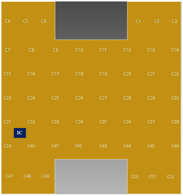
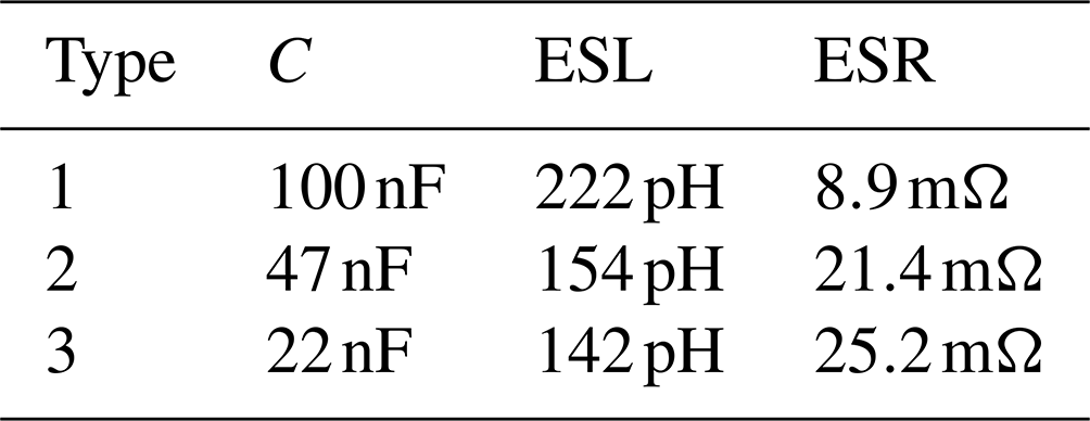
As in de Paulis et al. (2019), we work with three different types of decaps, which will be coded using the digits 1, 2, and 3 with corresponding values for capacitance C, equivalent series inductance ESL, and equivalent series resistance ESR as shown in Table 1. The decap types used in this example are commercially available and specifically developed for decoupling purposes. As a consequence, they feature a very low ESL.
The placement of these decaps on the PCB is restricted to a fixed grid with 52 positions. Additionally, the maximum number of decaps that can be placed on the PCB is limited to 10. In each run of the GA, the number of decaps to be placed is set to a particular value. Several runs of the GA are performed with an increasing number of disposable decaps in each subsequent run. The goal in this procedure is to optimize the placement of the given number of decaps to achieve the best possible decoupling performance. The latter is assessed via the input impedance of the PCB in frequency domain seen from the VCC pin of the IC that is marked by a blue rectangle in Fig. 1.
The general structure of an ANN is shown in Fig. 2. As reported by Ghafarian Shoaee et al. (2023), a vector of size 20 is used as the input layer of the ANN for each simulation depending on the number of decaps added and their type, and a vector of size 231 is used as the output layer representing the corresponding impedance values in equidistributed frequency points. The process of training an ANN requires the availability of a large amount of data. These can, e.g., be assembled from legacy data stemming from former design approaches. As such data are not available for the current study, a totality of 15 001 parameter sets is generated as data and labeled by impedance simulations. More precise, the frequency domain input impedance at the VCC pin of the IC, i.e., the impedance of the PCB seen from the IC, is computed for frequencies between 1 and 600 MHz to label the design parameters, i.e., decap positions and types, that are handed over to the ANN.
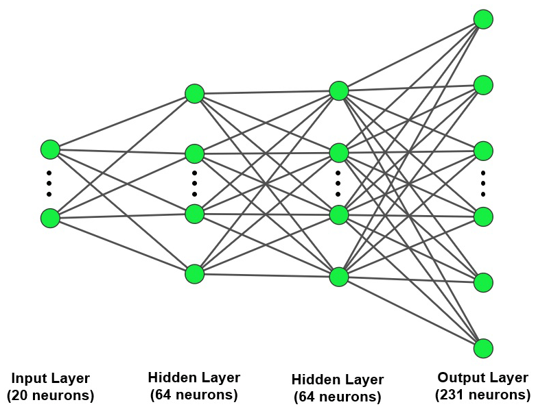
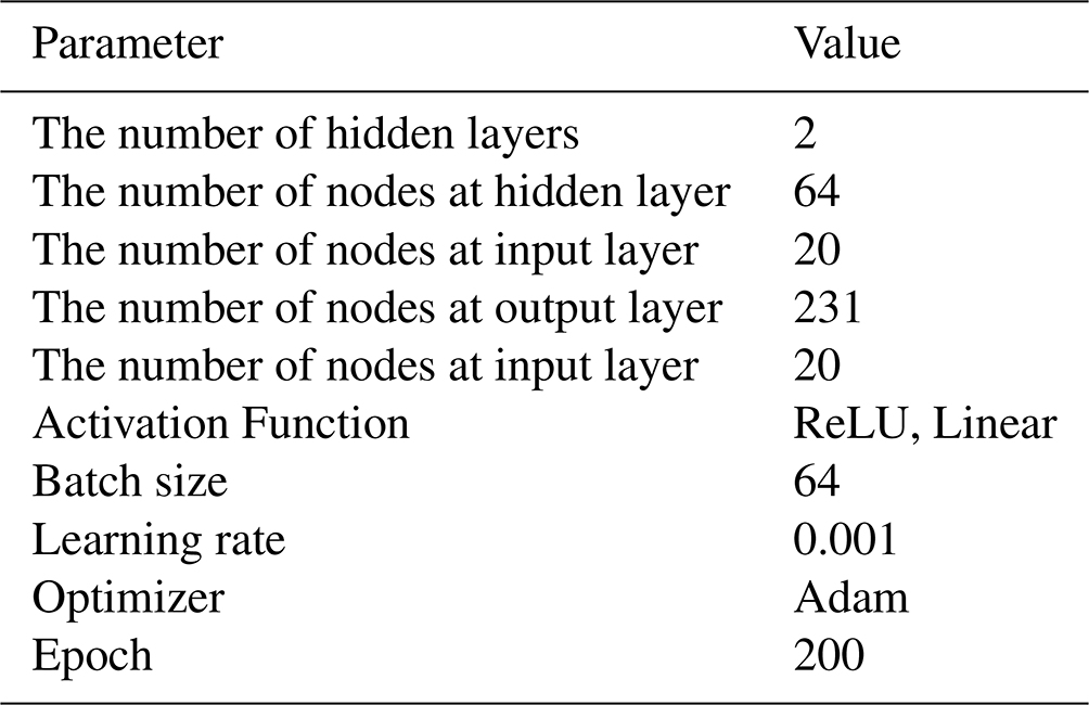
From the generated data, 80 % are used for training and 20 % for testing. After the ANN is optimally adjusted, a final check with the previously separated test data is carried out to guarantee that no overfitting has occurred, see, e.g., Zhou (2021), Tensorflow (2022). With the properly trained and tested ANN, the VCC input impedance can accurately be predicted for new input data (i.e., decap designs) and in addition classified. As a suitable ANN configuration, a network of 2 fully connected layers, each containing 64 nodes has been identified. The activation function used in this network is the rectified linear activation function (ReLU), which is a popular choice for deep learning tasks. The loss function used to measure the distance between the model predictions and the training labels is the Mean Squared Error (MSE). To test the trained ANN, the Mean Absolute Error (MAE) is chosen to have an independent performance metric for the ANN.
The learning rate is set to 0.001. This figure controls the step size used by the optimization method to make updates to the internal weights of the ANN aiming to obtain an optimal match between the model predictions and the training labels. Here, the Adam optimizer, a variant of the stochastic gradient descent, is utilized. It is widely used in deep learning and has been proven effective in various applications. The batch size for the optimizer is set to 64 and the number of training iterations or epochs equals 200. Table 2 summarizes the hyperparameters used.
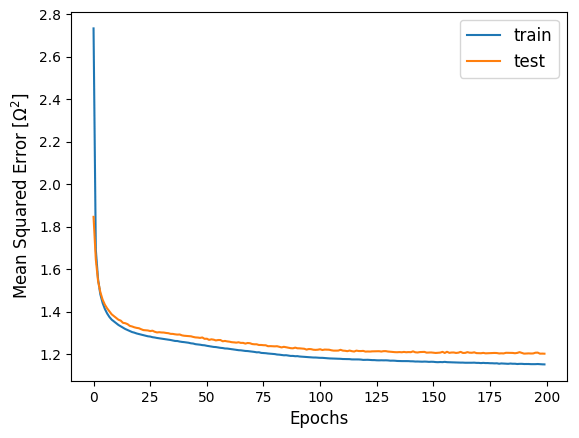
The entire training process takes less than 1 min. Figure 3 shows that, during training, the proposed ANN converges within less than 200 epochs to a low residual MSE value for both the training data (represented by the blue line in the Fig. 3) and the test data (represented by the red line in the Fig. 3).
The test results, measured using the MAE, are of similar quality (here not presented). The employed machine learning model has been validated by comparison of its performance with those of models with manually changed hyperparameters. Better results have been achieved by Ghafarian Shoaee et al. (2023) by an automated hyperparameter tuning via Bayesian optimisation.
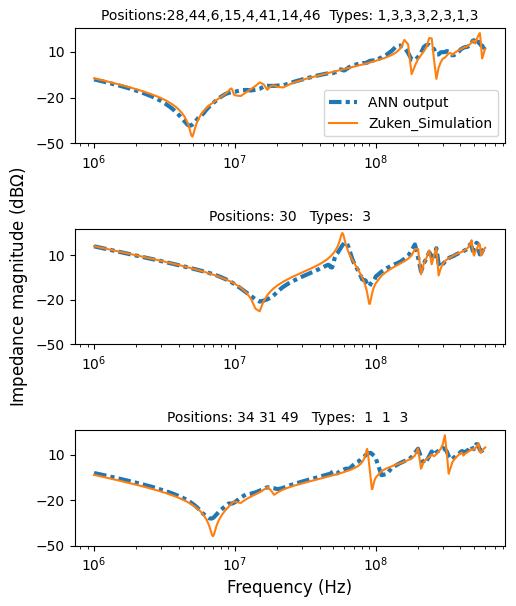
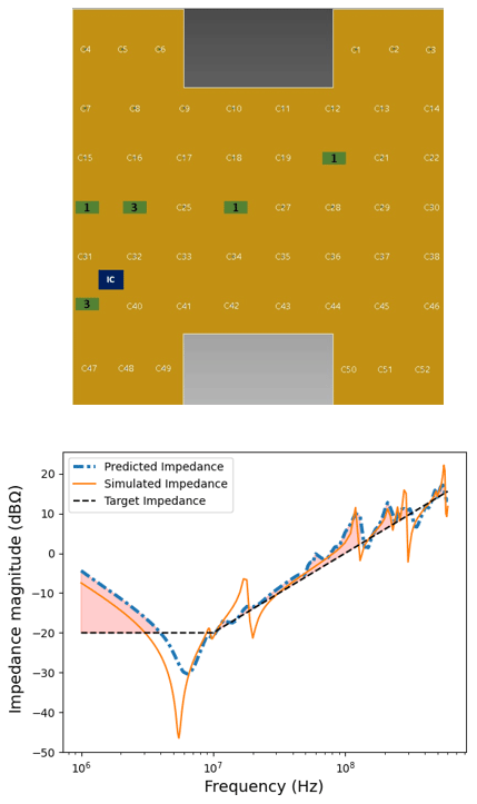
Figure 4Comparison of the input impedance at IC power pin predicted by the ANN and determined by simulation with eCADSTAR PI.
Comparing the output of the ANN with the simulation, it can be seen that it assesses the resonance frequencies correctly, but the predicted amplitudes are slightly lower. These results, combined with the strongly reduced computing time to obtain these results, justify the use of the proposed ANN to speed up the decap optimization process via a GA. Figure 4 shows the difference between the target curve and the ANN output for randomly picked examples from the test data.
The optimization procedure is based on a GA, whose architecture is tailored to the optimization of the placement of decaps on the PCB level. The decaps interact via two mechanisms with the PCB: First by influencing the frequency depending impedance according to their capacity, parasitic inductance ESL, and parasitic resistance ESR associated with a decap. The second aspect is the relative position of the decap with respect to the location of the IC's VCC pin, where the input impedance is evaluated. To identify a minimal set of decaps, the optimization process is repeated iteratively, starting with a small number of decaps and increasing it in each iteration. It stops either when the target is reached with a certain number of decaps or when the maximum number of decaps permitted by the designer is reached. Figure 5 shows all steps of the iterated GA.
In a GA, a certain number of individuals or chromosomes is gathered to a population. Each of these chromosomes contains encoded information about the positions, where a decap shall be placed, and its particular type. The fitness of all chromosomes is determined by the ANN via impedance computation for the particular designs that are encoded in the chromosomes. In this work, each chromosome is a vector of length 2n, if is the number of decaps employed. The first n entries are integers between 1 and 52 containing the numbers of the grid points where the decaps are located, and the following n contain the code of the corresponding type, an integer between 1 and 3. In the following, we will discuss the components of the GA and explain how we have tailored these components to our application.
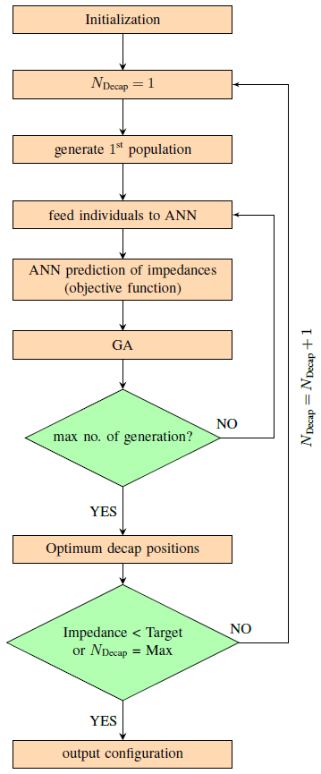
Figure 5Flow chart of the iterated GA approach with validation of the fitness function by an ANN.
3.1 Initialization and competitive selection
According to physical evidence, the initialization of the population in the GA can be done with individuals randomly selected from a pool of candidate solutions placed near and around the IC with the aim to accelerate the subsequent optimization process. After a population has been set up, in each generation, a set of individuals is selected from the population, their fitness values are compared, and the genes of the best individual are copied into the mating pool. This process is repeated several times until a certain number of individuals is present in the mating pool. The number of chromosomes taken into the mating pool can be used to adjust the selection pressure – the more individuals are selected, the greater the selection pressure.
3.2 Recombination/crossover
Cross-over is one of the steps in the GA, where two chromosomes interact to create a third, potentially better chromosome. The two chromosomes involved are called parent chromosomes, while the newly created chromosome is called a child. The child inherits some traits from the first parent and other traits from the second parent. The percentage of inheritance from each parent is determined by the location of the crossover, which is randomly chosen. There are different crossover methods. In this work we have chosen the One-Point Crossover: The crossover point is determined by a random number, at which the two parents are cut. The first of the two offsprings produced receives the first part of the chromosomes from the first parent and the second part of the second chromosome. The second offspring receives the complementary genes, i.e., the first part of the second and the second part of the first parent.
We use a one-point crossover method that is particularly tailored to our case. As the first half of the entries to our chromosoms refers to spatial information, and the second half to its type, we apply a one-point crossover to both parts separately, as illustrated in Fig. 6
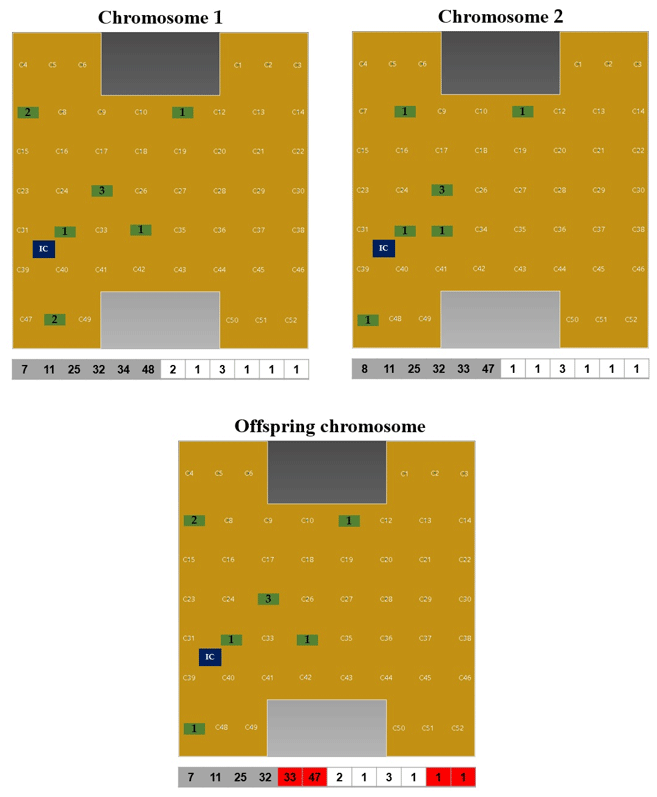
Figure 6The crossover of parent chromosome 1 and parent chromosome 2 leads to an offspring chromosome that exchanges the positions of 34 and 48 from parent 1 and 33 and 47 from parent 2.
3.3 Mutation
Genetic algorithms have a tendency to converge towards local optima rather than the global optimum of the problem. To prevent getting stuck in a local optimum and missing the global optimum, random changes are introduced in the offspring that are produced after crossover. These random changes are called mutation. Mutation causes a random change in the chromosome and thus a change in the design it encodes. Smaller changes increase the probability that the chromosomes converge, but the convergence is more likely to be towards a local optimum. On the other hand, larger changes increase the probability that the solution converges towards a global optimum, but at the expense of a worse convergence rate. The probability of a mutation occurring, the mutation rate, can be controlled in order to reduce the chance of convergence to a local optimum.
A simple example of mutation is shown in Fig. 7. A randomly selected capacitor changes its position from grid point 28 to grid point 36 and its type from 1 to 2.
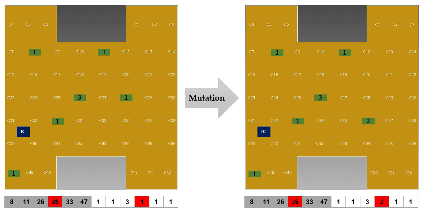
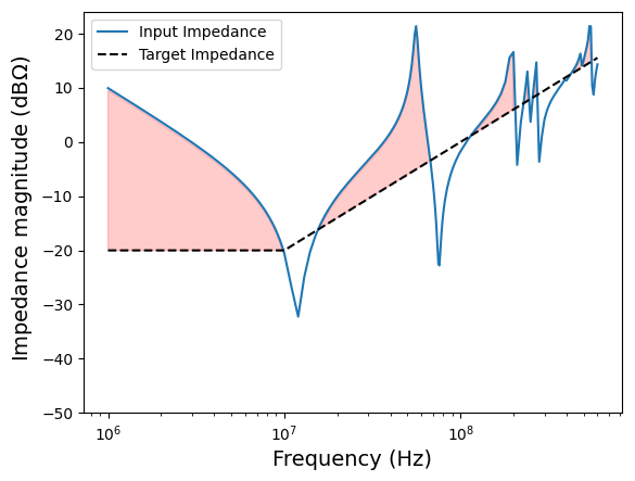
Figure 8Fitness function represented as area above an arbitrary target function (dashed line).
3.4 Fitness function
The fitness calculation for the optimization process is done through a fitness function. The fitness function is used to measure the deviation between the input impedance predicted by the ANN at one VCC connections and the target impedance.
This deviation represents the actual performance of the ANN, with lower deviation indicating a better fit or fitness for the problem. By minimizing this deviation, the fitness function helps to identify the best possible placement of decaps on the PCB that achieve the best impedance performance.
We determine that part of the area between the preview of the frequency depending input impedance magnitude and the target impedance ZT=ZT(f), where the input impedance lies above the target function, as show in Fig. 8, by using the following fitness function:
with
Here, fi are fixed frequency points in which the prognosis on the input impedance is formulated by the ANN.
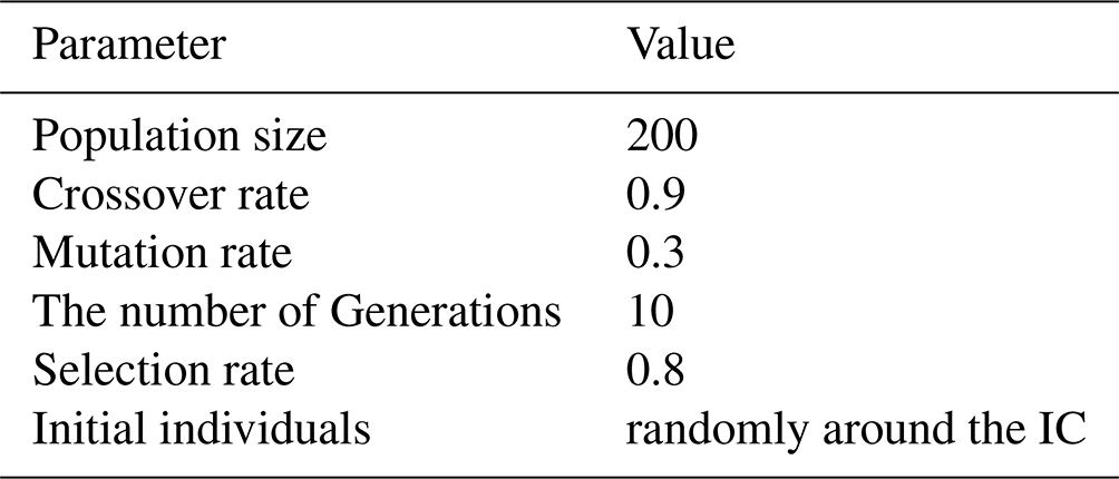
The GA operates on a population size of 200 individuals, with crossover rate of 0.9, mutation rate of 0.3, and a total of 10 generations. These parameters are used to control the behavior of the GA during the optimization process. The population size represents the number of individuals in each generation, the crossover rate controls the frequency of combining genetic information from different individuals, the mutation rate determines the probability of introducing random variations in the genetic information, and the number of iterations represents the number of cycles the algorithm will run before stopping. These parameters (Table 3) are set in order to achieve the best results for the specific optimization problem.
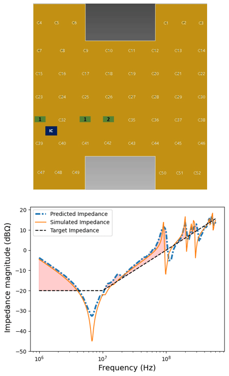
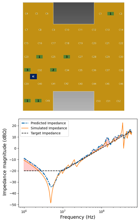
Figures 9 to 11 shows the optimal solution of the GA algorithm after placing 3, 5, and 7 decaps. We can clearly see an improvement in the GA solution after each iteration, that is, after the insertion of a new decap.
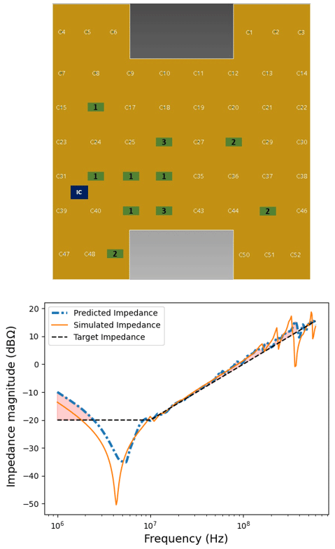
With 10 decaps placed to optimum positions, we observe in Fig. 12 that the GA solution is close to the target impedance.
As we see in Fig. 13 the GA finds a solution with 10 decaps that is very close to the curve obtained with 52 decaps (of random type). For some frequencies, it even provides a better result. This is not surprising, since increasing the number of the decaps can deteriorate the PCB impedance at certain frequencies due to the limited band width of the capacitive effect of the decaps and their parasitic inductance. For these reasons, locally operating capacitors are more efficient than an across-the-board approach. In addition, the GA efficiently saves resources by providing an optimal solution with a minimal number of decaps, coincidentally satisfying the constraints with respect to the given target impedance.
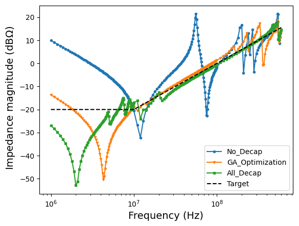
Figure 13Comparison between the results of the PI-simulations of the GA-optimal solution with 10 decaps and the solution with and without 52 decaps.
Although it is in general not possible to be sure that an optimum position has been reached, the results show that a GA can perfectly be used as an efficient heuristic to come to solutions that fulfill given requirements. Of course, subsequent tests if the identified candidate fulfills the requirements as done in this work are mandatory. A comparison of the findings of the GA with manually identified designs reveals that the optimal GA solution shows slightly better performance compared to a manually adjusted solution: Moving the capacitor from C34 to C32 or from C20 to C33, would slightly worsen the impedance profile, as has been checked.
In conclusion, the placement and dimensioning of decaps using an optimization algorithm, in this case a Genetic Algorithm, has been successfully implemented. The use of a surrogate model significantly reduces computation time. Hence, the risk of a redesign that would take several weeks can be reduced by a computation that just needs a few minutes. The GA experiments were run on a workstation with 1 Intel Core i9-11980HK CPUs @ 2.30 GHz, with 16 cores, and 32 GB RAM and took 20 min. However, the computation time for the GA is still relatively long and depends on the GA's hyperparameters. To validate the GA, it is essential to run a simulation again with a PI check at the end.
Looking ahead, the established link from a commercial tool for data generation to a powerful, but data intensive optimization framework via training of a fast and adaptive ANN surrogate model opens up the way to deal with complex state of the art scenarios like multi-layer PCBs with multiple power/ground pins and IC package PDNs. For such PCBs capacitors may not only be placed on the top layer near the IC, but also on the bottom layer, directly under the IC power pins. The ANN surrogate model can be modified using a 2D-Convolutional Neural Network (CNN) to represent top and bottom PCB layers with decap types encoded by different colors. For including IC packages, a 3D-CNN can model the entire PCB with colors coding decaps, layers, packages, and vias. Additionally, a multi-objective GA can optimize multiple impedance targets on numerous pins effectively. A thorough analysis of the algorithm's usability when applied to slightly modified PCB structures (transfer learning) as well as simplifications with regard to the consideration of more sophisticated physical model designs as done in this work (in the sense of physics-informed ML) will be treated in subsequent work.
Due to project restrictions, the source codes and datasets are not publicly available. For more information, please contact the main author.
ZN developed the idea to this work, designed the scientific study, programmed the genetic algorithm as well as scripts for data transfer, produced the graphical representation of the results, and wrote most of the text. NGS generated the required data and supported the programming. MS consulted the team, discussed methods and results, and revised the text.
The contact author has declared that none of the authors has any competing interests.
The responsibility for this publication is held by the authors only.
Publisher's note: Copernicus Publications remains neutral with regard to jurisdictional claims made in the text, published maps, institutional affiliations, or any other geographical representation in this paper. While Copernicus Publications makes every effort to include appropriate place names, the final responsibility lies with the authors.
This article is part of the special issue “Kleinheubacher Berichte 2022”. It is a result of the Kleinheubacher Tagung 2022, Miltenberg, Germany, 27–29 September 2022.
This work is funded as part of the research project progressivKI (https://www.edacentrum.de/projekte/progressivKI, last access: 26 July 2024) in the funding program NFST by the Bundesministerium für Wirtschaft und Klimaschutz (BMWK) of the Federal Republic of Germany (grant no. 19A21006/R/O).
This paper was edited by Dirk Killat and reviewed by four anonymous referees.
Archambeault, B.: Effective power/ground plane decoupling for PCB, IEEE Video Distinguished Lecturer Program, 2007. a
Barnes, H.: Power Integrity Target Impedance Says it All, Power Delivery is AC not, in: Keysight/ADS Workshop, 14thAnnual Central PA Center for Signal Integrity Symposium, 16 April 2021, Penn State Harrisburg, 2021. a
Chen, J. and He, L.: Efficient in-package decoupling capacitor optimization for I/O power integrity, IEEE T. Comput. Aid. D. 26, 734–738, 2007. a
Chuang, .-H., Guo, W.-D., Lin, Y.-H., Chen, H.-S., Lu, Y.-C., Cheng, Y.-S., Hong, M.-Z., Yu, C.-H., Cheng, W.-C., Chou, Y.-P., Chang, C.-J., Ku, J., Wu, T.-L., and Wu, R.-B.: Signal/power integrity modeling of high-speed memory modules using chip-package-board coanalysis, IEEE T. Electromagn. C., 52, 381–391, 2010. a
de Paulis, F., Cecchetti, R., Olivieri, C., Piersanti, S., Orlandi, A., and Buecker, M.: Efficient iterative process based on an improved genetic algorithm for decoupling capacitor placement at board level, Electronics, 8, 1219, https://doi.org/10.3390/electronics8111219, 2019. a, b
Ghafarian Shoaee, N., Nezhi, Z., John, W., Brüning, R., and Götze, J.: Generating AI modules for decoupling capacitor placement using simulation, Adv. Radio Sci., 21, 49–55, https://doi.org/10.5194/ars-21-49-2023, 2023. a, b
Juang, J., Zhang, L., Kiguradze, Z., Pu, B., Jin, S., and Hwang, C.: A modified genetic algorithm for the selection of decoupling capacitors in pdn design, in: 2021 IEEE International Joint EMC/SI/PI and EMC Europe Symposium, 26 July 2021–13 August 2021, Raleigh, NC, USA, pp. 712–717, IEEE, 2021. a
Lu, T., Sun, J., Wu, K., and Yang, Z.: High-speed channel modeling with machine learning methods for signal integrity analysis, IEEE T. Electromagn. C., 60, 1957–1964, 2018. a
Smith, L. and Bogatin, E.: Principles of Power Integrity for PDN Design–simplified: Robust and Cost Effective Design for High Speed Digital Products, Prentice Hall modern semiconductor design series: Prentice Hall signal integrity library, Prentice Hall, ISBN 9780132735568, 2017. a
Swaminathan, M., Chung, D., Grivet-Talocia, S., Bharath, K., Laddha, V., and Xie, J.: Designing and modeling for power integrity, IEEE T. Electromagn. C., 52, 288–310, 2010. a
Tensorflow: Hyperparameter Tuning with the HParams Dashboard, Tech. rep., Tensorbord, https://www.tensorflow.org/tensorboard/hyperparameter_tuning_with_hparams (last access: 26 July 2024), 2022. a
Wu, T.-L., Chuang, H.-H., and Wang, T.-K.: Overview of power integrity solutions on package and PCB: Decoupling and EBG isolation, IEEE T. Electromagn. C., 52, 346–356, 2010. a, b, c, d, e, f
Zhou, Z.-H.: Machine learning, Springer Nature, in: Neural networks, 103–128, 2021. a
Zuken: eCADSTAR, Tech. rep., Zuken, https://www.zuken.com/us/product/ecadstar/ (last access: 26 July 2024), 2023. a