 | 01 Dec 2023
Hybrid integrators with predictive overload estimation for analog computers and continuous-time ΔΣ modulators
Dirk Killat
Bernd Ulmann
Sven Köppel
Continuous-time integrators are a central component in ΔΣ modulators, in analog computers, and general analog signal processing. If several integrators are interconnected, scaling plays an important role: In analog computers, scaling is performed with respect to the machine unit (MU). In ΔΣ modulators, scaling is performed in such a way that at maximum input signal the allowable dynamic range of no integrator is exceeded. In both cases the scaling is a compromise limiting the dynamic range.
For analog computers, it was proposed early on to extend the dynamic range by hybrid integrators. Here, an analog range overflow is processed digitally and the analog integrator is reduced to its permissible operating range within the machine unit interval. While in earlier proposals for hybrid integrators only the subsequent integrator stage processes the overflow and works with reduced analog values, our hybrid integrator can process the overflow directly, with the analog reset process being continuous-time.
In the case of highly dynamical input signals and transients, analog overload handling is further improved by a prediction of the overload that includes the currently applied input signal in the calculation. For example, with continuous-time ΔΣ modulators, overload of the analog integrator can be reliably avoided.
- Article
(7222 KB) - Full-text XML
- BibTeX
- EndNote


Analog continuous-time (CT) integrators are a fundamental building block in analog computers (Howe, 2005), in continuous-time ΔΣ ADCs (Ortmanns and Gerfers, 2006), in robust analog controllers (Jin et al., 2022), and many other analog signal processing circuits. Analog computers are popular for solving and simulating differential equations, which usually involves connecting integrators in series, typically with some sort of feedback loop. The series of integrators in ΔΣ modulators makes it possible to achieve higher-order noise shaping and, accordingly, to reduce the quantization noise in the signal band.
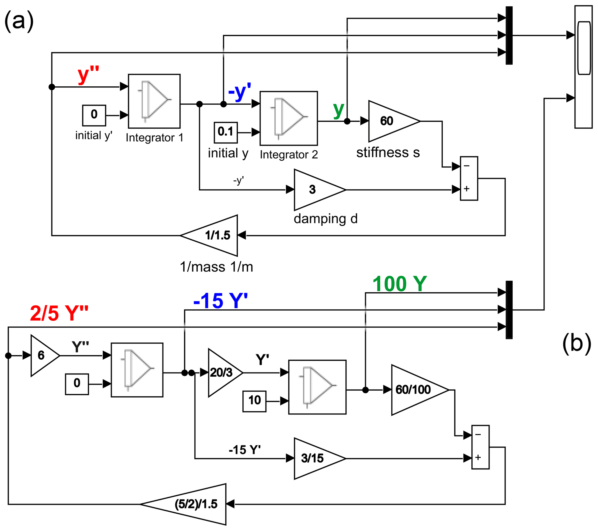
The problem of amplitude scaling will be illustrated in the following by a spring-mass damper system (Hall and Kahne, 1970; Ulmann, 2022; Navarro, 1962): Let the system have a spring stiffness of 60 kg s−2, a damping coefficient of 3 kg s−1, a mass of 1.5 kg, and an initial displacement of 0.1 m. A Matlab-Simulink model for this is shown in the upper part of Fig. 1.
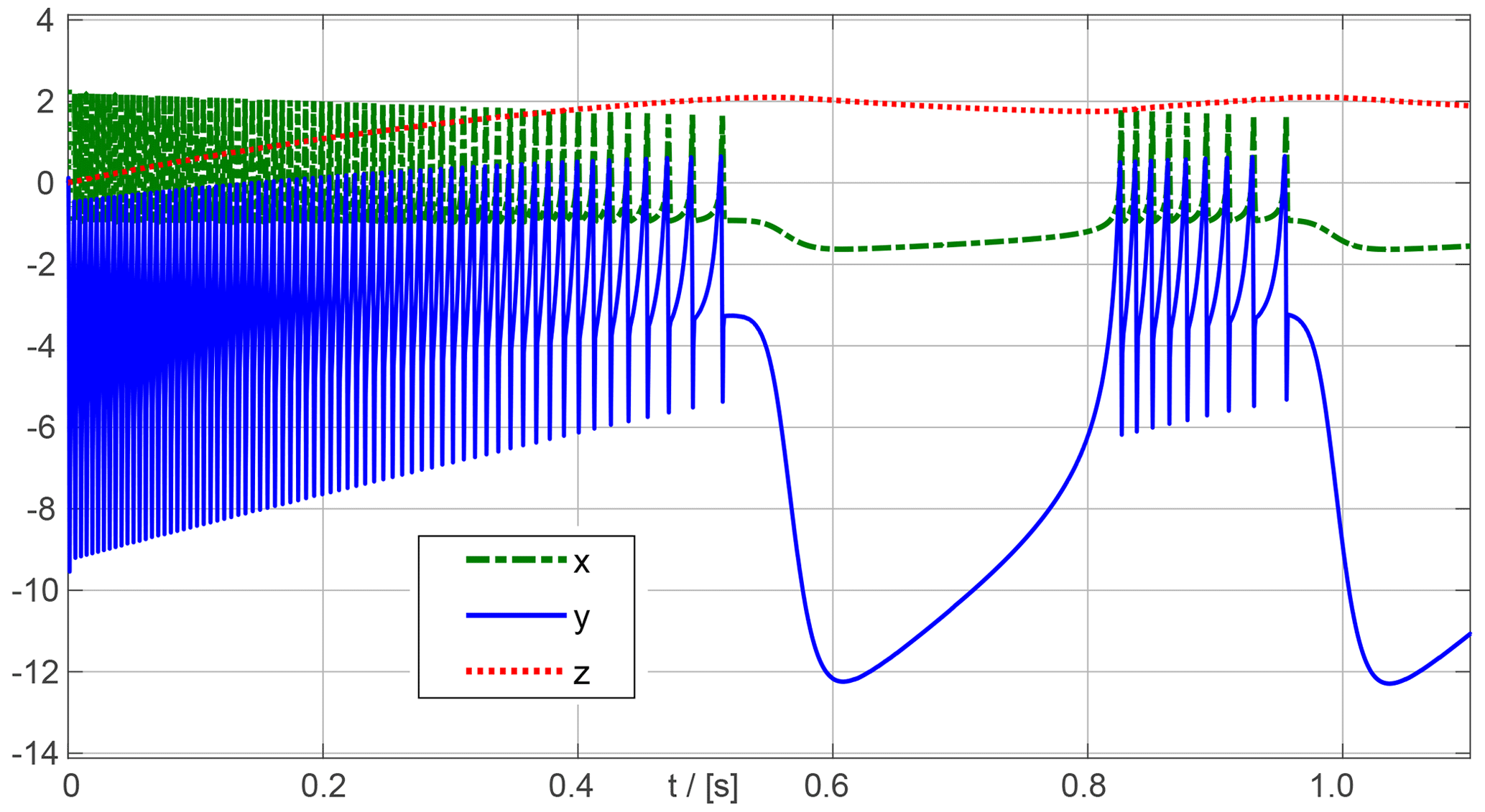
The simulation result of the unscaled differential equation is shown in Fig. 2a.
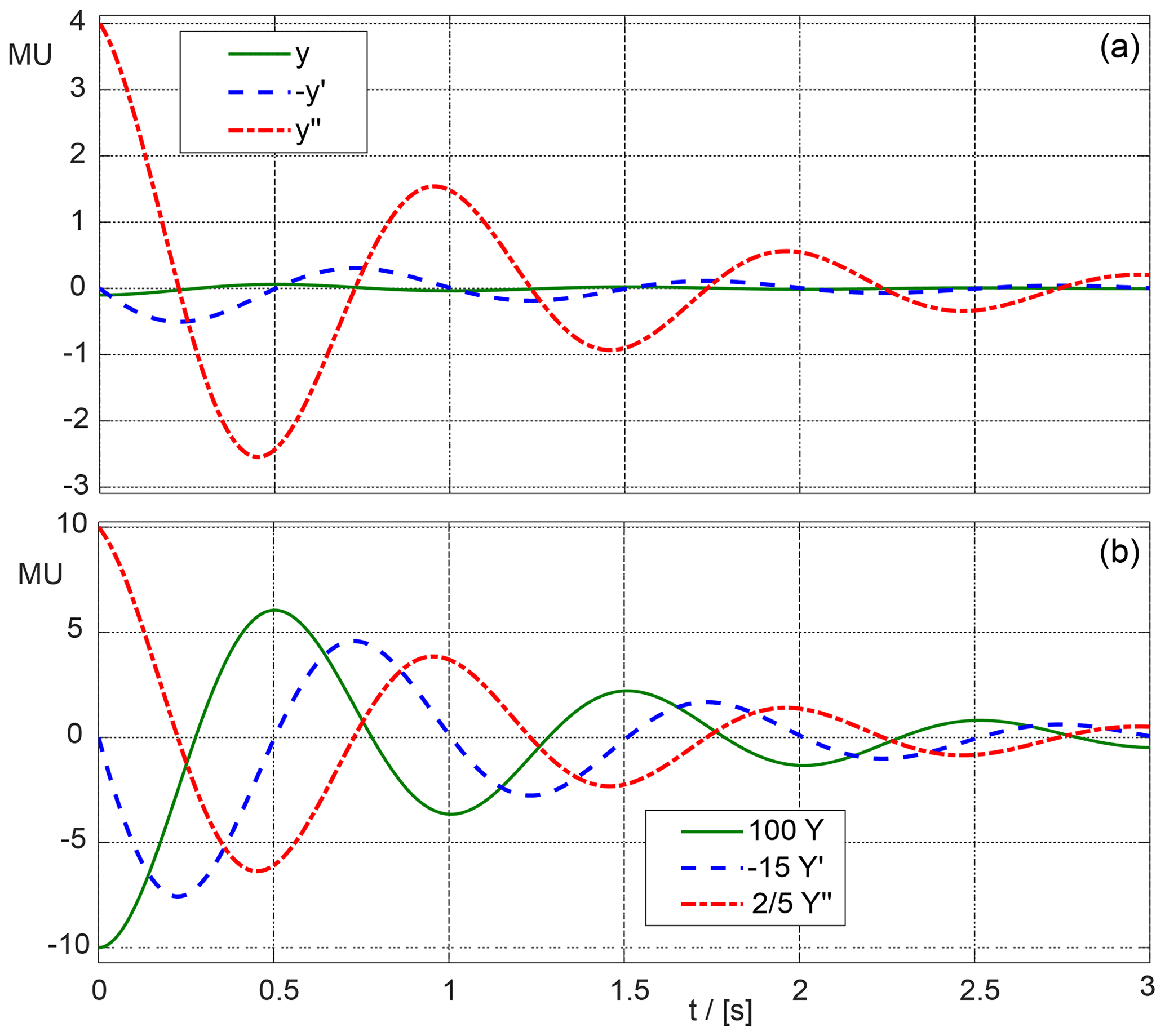
It can be seen that , , and y are scaled unevenly, i. e., the dynamic range is not used optimally. To optimize the problem for the hardware of an analog computer, the amplitude range of the quantities must be scaled to the machine unit (MU). In modern discrete analog computers the machine unit can be e.g. 10 V (Ulmann et al., 2021), so that the amplitudes of the signals should be as close as possible to the 10 V, but the 10 V must not be exceeded. For scaling, experience with the implemented mathematical equation is required, or one can try to optimize the scaling experimentally. A solution for scaling to 10 V would be the substitution , and y⇒[100 Y]. To scale the model, , d, and s are multiplied by the reciprocal scaling factors. In addition to that, the integrators must be scaled as well at their inputs (Fig. 1 below). The simulation of the model scaled to 10 V is shown in Fig. 2b.
In addition to amplitude scaling, scaling in the time domain can also be performed. This is used to adapt the mathematical task to the bandwidth and slew rate of the electronic circuit components. Time scaling adapts the real time of the simulated model (also called wall clock) to the simulation or machine time. Thereby the simulation time can run faster or slower than the wall clock time.
The hybrid integrator solves the problem of amplitude scaling. The time scaling is independent of this. However, very different time constants in a mathematical problem also lead to problems with amplitude scaling, so that the hybrid integrator can also be used to an advantage in such cases.
The operation of scaling in ΔΣ modulators is shown in Fig. 3, showing a 3rd order modulator with distributed feedback and 1-bit quantizer. In the chain of integrators, the amplitudes must be scaled down by a factor towards the end, as exemplified by the 3rd integrator. There are two main reasons for this: In the case of the 3rd order modulator, stability is improved because the gain gq of the linearized 1-bit quantizer increases and only then the modulator becomes conditionally stable (see, e.g., Ortmanns and Gerfers, 2006, Chap. 2.7.4). Another and decisive reason for scaling in ΔΣ modulators is the necessity to limit the signal amplitudes to the practical dynamic range of the analog integrators.

By downscaling the signal amplitudes the actually achievable signal-to-noise ratio is reduced. Therefore, attempts have already been made to both increasing the stability of the modulator and increasing the dynamic range (Au and Leung, 1997; Shim et al., 2005a, b) by local detection of the overflow at the individual integrators of the modulator, a subsequent AD conversion of the overflow, and a local negative feedback directly at the integrator.
Section 2 of this paper reviews the principle of the hybrid integrator originally designed for analog computers, explains the basic operation of the hybrid integrator, and presents its fundamental drawback. In Sect. 3, the hybrid integrator with CT reset presented in (Killat et al., 2022) is compared in detail with previous solutions. In Sect. 3.2, a new range overflow estimation is introduced that optimizes the dynamic range, especially for transient input signals or use in ΔΣ modulators. In Sect. 4 the operation of the hybrid integrator with CT reset and with overload estimation is illustrated by examples.
The first approach to hybrid integrators was presented in Skramstad (1959) and was the starting point of subsequent work by Wait (1963); O'Grady (1966). At that time, the emphasis was on extending the dynamic range for the solution of differential equations. The devices available at that time hardly allowed a capacitive reset as proposed in the integrated solution of Bryant et al. (2012). Therefore, the overflow from the analog integrator to the digital counter had to be realized by a time-continuous compensation in the subsequent hybrid stages of the integrators, which works well for classical problems like spring-mass-damper systems or harmonic oscillators due to the negative feedback of the integrators and is therefore often used as an example for the functionality of hybrid integrators in papers of that time.
2.1 Hybrid integrator basics
First we describe the basic principle of hybrid integration according to Skramstad (1959):
The integrator integrates the input variable X over time t with initial value Y(0). T is the time constant of the integrator:
In the hybrid integrator, the integration variable X and the integral Y are decomposed into an analog and a digital component:
Thus, the analog and digital components of X are integrated. The initial values are also divided into analog YA(0) and digital YD(0) components:
The integral over the analog XA and digital component XD of X can be decomposed into a sum, an instantaneous term and an integral over time t. The digital component is integrated in multiples of the time interval Δt. The instantaneous value of the integral in the nth time interval is:
here XD(i) is the value of XD in the ith time interval. Assuming that the initial values YD(0) and YA(0) are both 0, Fig. 4 shows the integral of Eq. (5). The summand with index i=0 to n−1 is the Integral 1 in Fig. 4. The second term XD(n−1)τ is the instantaneous value of the digital integral in the time interval and denoted Integral 2 in Fig. 4. The third term, the analog part of the integral, is Integral 3.
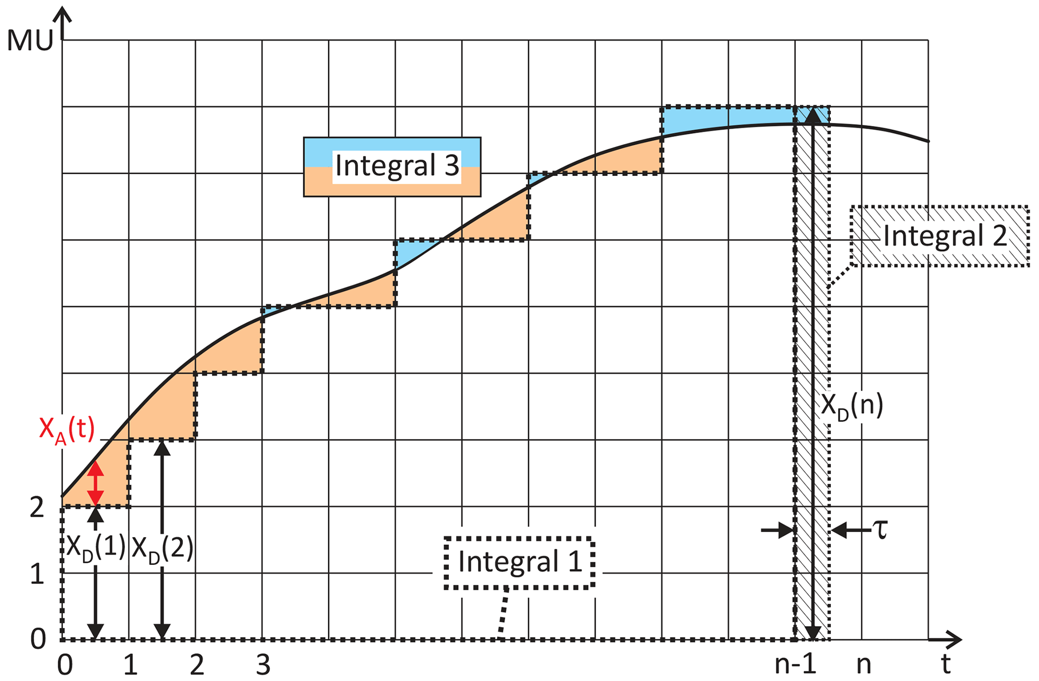
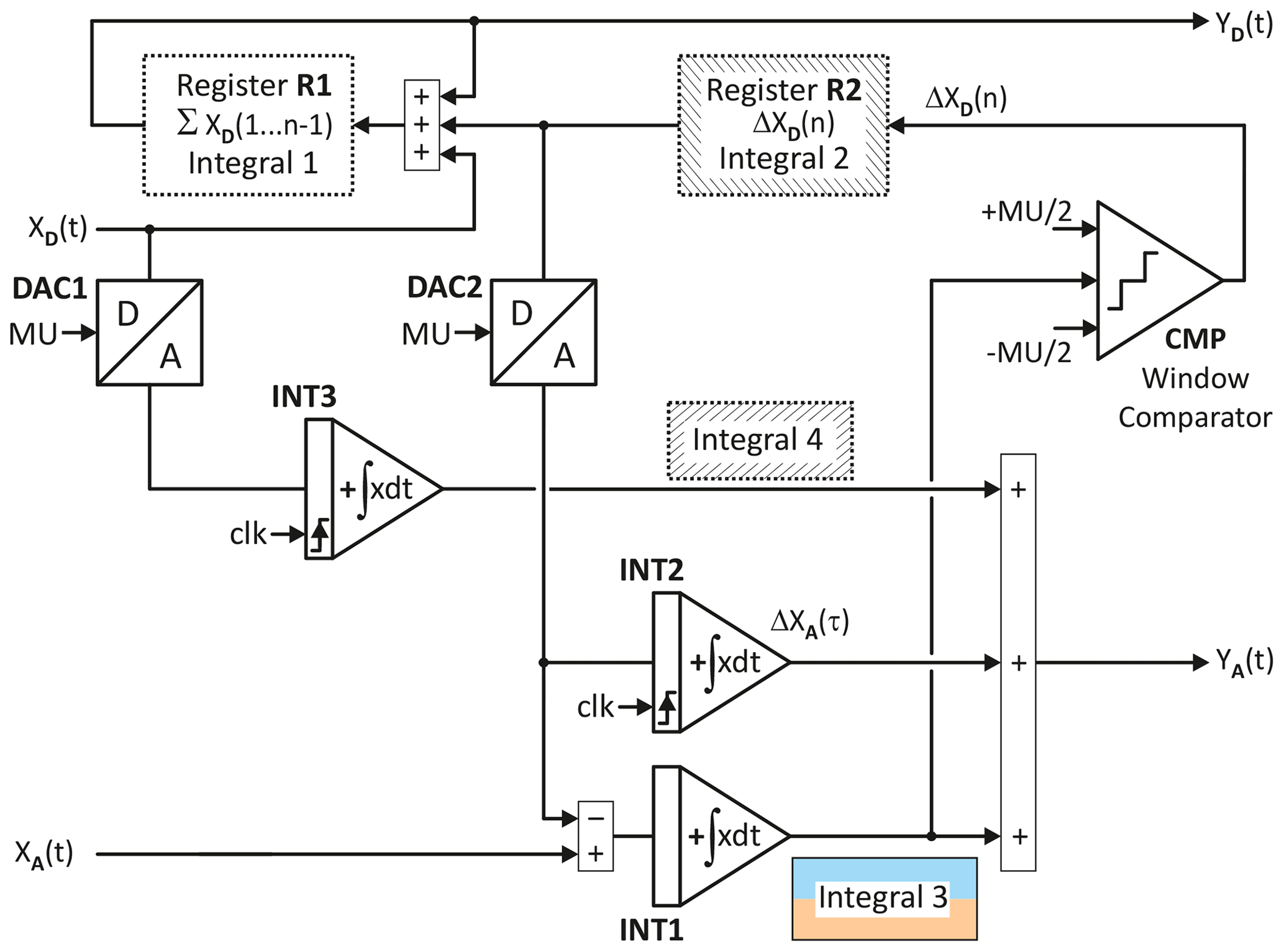
Figure 5 shows the block diagram of the hybrid integrator according to Skramstad (1959). The digital part consists of two registers R1 and R2. R1 represents the Integral 1, that accumulates with each clock, at each time step nΔt, the value XD(n−1) from the register R2 and the change . This change is generated by a window comparator with thresholds MU (MU, machine unit). The digital value of Integral 1 is DA-converted by DAC1, added up with other analog components of the integral and then fed to the analog output YA of the integrator. Since YA(t) is supposed to represent the analog part of the integral without the digital part, DAC1 gets the −MU as reference for Integral 1.
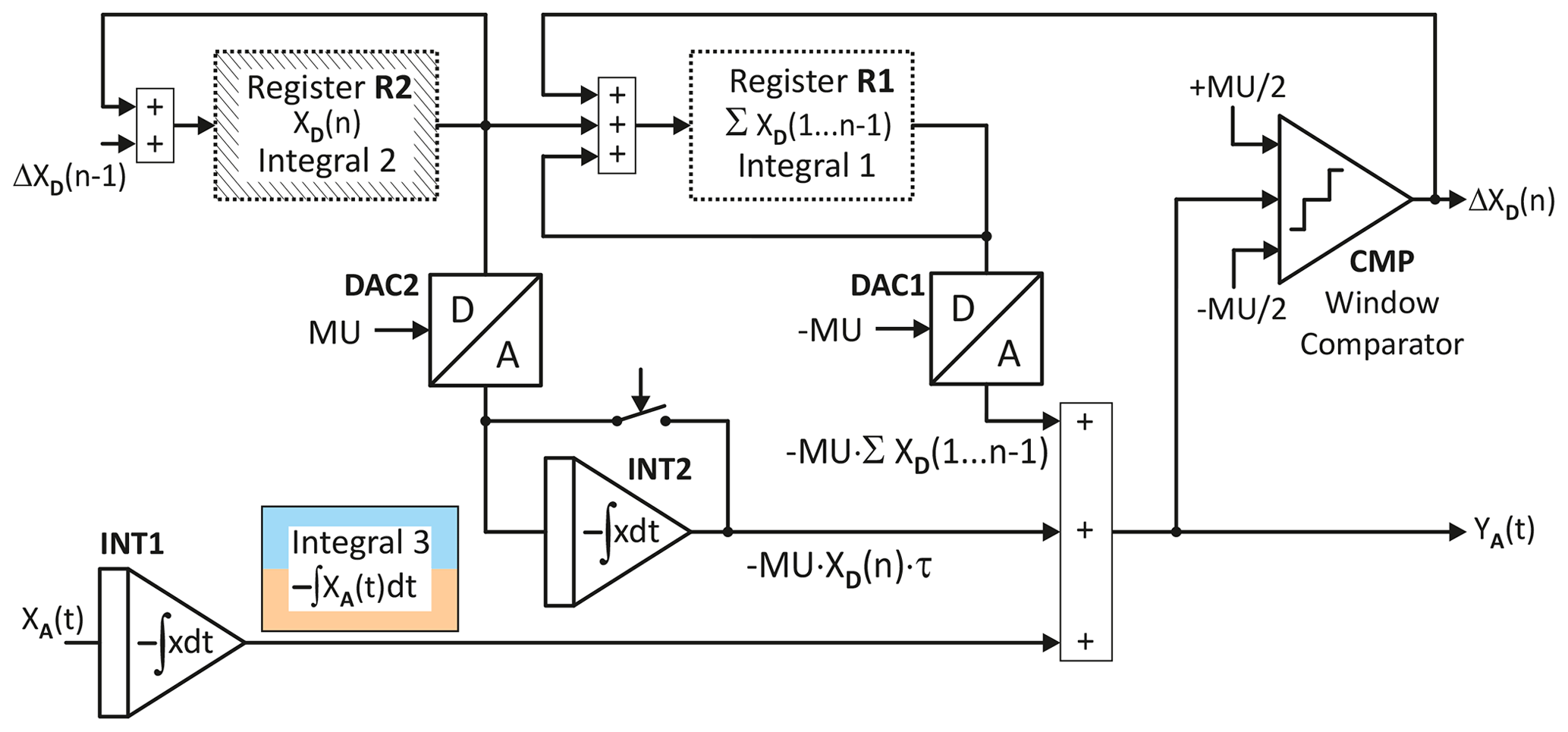
The value XD(n−1) of the register R2 is transferred via DAC2 with +MU as reference to an integrator INT2, which is periodically reset at the instants nΔt. This generates a saw-tooth voltage representing the instantaneous value of Integral 2, which is added to the output YA by means of a summer.
The analog portion of Integral 3 with input XA(t) is integrated and added directly to YA. Assuming that XA(t) corresponds to YA(t) of the previous integrator stage, and that YA(t) is obtained by subtracting the digital part of Integral 2, Integral 3 is the color-coded area in Fig. 4. It may become positive or negative. If several hybrid integrators are concatenated and fed back, as is the case when solving differential equations in analog computers, Integral 3 is indirectly minimized in the individual hybrid integrators by keeping YA(t) small in size by subtracting the digital parts of the total integral.
2.2 Disadvantage of the previous hybrid integrator
From Fig. 5 it can be seen that the hybrid integrator has no local feedback, i. e. if YA(t) exceeds MU, this is added to Integral 1 and the analog output YA(t) is reduced in amount accordingly, but the value of integrator for Integral 3, i. e., the actual analog integrator, is not reduced in amount. The reduction occurs indirectly when the chain of integrators is fed back eventually.
The operation and efficiency of the hybrid integrator presented so far is demonstrated in Skramstad (1959); Wait (1963); O'Grady (1966) on examples with feedback, i. e., by means of using differential equations such as or . For general applications in analog computing or instrumentation, the previous hybrid integrator does not allow to constrain the actual analog integral of the hybrid integrator, because a local feedback on the analog integrator component is missing.
The issue of a hybrid integrator requiring local feedback is addressed in Bryant et al. (2012). Here, a partial capacitive reset of the integrator is performed when a window comparator exceeds its thresholds. The problem is that the reset does not have an ideal voltage waveform, i. e., the digital portion of the hybrid integrator does not match the corresponding analog portion just after the reset signal. While this can be systematically taken into account in CT-ΔΣ-modulators by the Laplace transforms of the feedback DAC, and only influences the noise shaping, the non-ideal voltage curve in the switched-capacitor-based reset of the hybrid integrator leads to errors in the result of an analog computing circuit.
In Tsividis and Guo (2015) it is proposed to avoid a capacitive reset by reversing the integration direction when a reference threshold voltage is exceeded. A disadvantage of this method are the required continuous-time comparators, which have to detect an overflow of the integrator asynchronously. By reversing the direction of integration, a reset can be avoided, but the accuracy of the threshold of the continuous-time comparators is crucial for the transfer from the analog integrator to the digital counter.
Based on Bryant et al. (2012), a partial reset of the analog integrator will be realized when the range of the window comparator CMP is exceeded. The reset will be realized by a continuous square wave signal instead of a switched capacitor circuit. This subsequently requires further compensation to represent the correct timing characteristics of the integrator when the digital part of the hybrid integrator switches.
3.1 Operating principle of new hybrid integrator
The improved hybrid integrator with local feedback is shown in Fig. 6. The corresponding integrals of the analog and digital parts of the total integral are depicted in Fig. 7. The digital portion of this total integral, Integral 1, is held in register R1. This register sums the digital input XD and ΔXD and represents the digital portion YD of the current hybrid value of the integrator.
The improved hybrid integrator requires three analog integrators INT1 to INT3, two of which are periodically reset by the clock. The integrator INT1 forms the analog Integral 3. Its output is given to a window comparator CMP, which generates the digital overflow ΔXD when the thresholds are exceeded, which is then DA-converted with +MU as a reference in DAC2 and then negatively fed back to the analog input of the integrator INT1 for Integral 3. Since the window comparator directly measures Integral 3 and since there is negative feedback in the case of digital overflow, this improved hybrid integrator achieves a constraint on the analog Integral 3 even without arranging the hybrid integrator in a loop, unlike the solutions shown in Skramstad (1959); Wait (1963); O'Grady (1966).
The digital overflow results in a linear characteristic of the reset of Integral 3. However, because the overflow is not yet stored in the digital output register R1 with the value Integral 1, the linear reset must be compensated with an opposite ramp ΔXA(τ) provided by the analog integrator INT2. This ensures that at each time represents the correct value of the hybrid integral.
If a digital overflow XD is present at the input of the hybrid integrator, it will only be taken into account in the following clock cycle of the register for Integral 1 and must therefore be DA-converted with DAC1 and then fed to the sum YA with integrator INT3 to obtain the correct total integral Y at any time.
Figure 7 shows the composition of the integral. Integral 1 is identical to the previously shown hybrid integrator. Integral 2 in the improved hybrid integrator no longer has the current analog represented value of XD(n)τ, but only the value ΔXD(n)τ, which certainly simplifies the scaling of the summation. To obtain the correct instantaneous value for a digital input quantity, the digital input XD must be integrated analogously and fed to the analog output component YA(t). This component corresponds to Integral 4.

The analog output YA(t) consists of three signals, Integral 3, the sawtooth shaped compensation of the time-continuous reset with ΔXA(τ), and the analog representation of the digital input of Integral 4. Integral 3 and ΔXA(τ) are smaller in magnitude than the machine unit (MU). Integral 4 also has a sawtooth shape, but can exceed 1 MU and reach XD(t)Δt at its peak. If YA(t) must be explicitly generated with a summer and represented as a voltage, the fraction represented by Integral 4 limits the dynamic range. However, if the hybrid integrator is followed by another stage with a hybrid integrator, the three components of YA(t) are fed into the following analog part of the hybrid integrator via separate resistors, so that the dynamic range is not limited, because the sum signal YA(t) does not occur explicitly as a voltage. Instead the sum is formed by the summer circuit of the following analog integrator.
Figure 8 shows the signal waveforms of the hybrid integrator.

First we consider the left side of Fig. 8 where a constant input signal XA(t) is present. The analog integrator signal ∫XA(t)dt reaches a maximum of MU (with MU=1) and then integrates back to zero level. To obtain the correct value of the analog component in the time domain from t=1 to t=2 in the presence of the continuous-time reset, the value XD(n) from register R2 is AD-converted and integrated with INT2 and then added to the analog integral as a ramp signal ΔXA(τ). Without this ramp signal ΔXA(τ) the value of the total integral in the phase of the continuous-time reset would not represent the correct value, as shown by the hypothetical waveform of in the lower part of Fig. 8.
On the right side of Fig. 8 the input signal is switched off at t=2.5 and again at t=3.5. The final values of the total integral are and 1.75. The comparator CMP switches at t=1 and, if the input signal is present until t=3.5, again at t=3 (red mark). Therefore the digital sum signal first reaches the value 1 and then the value 2. The final values of the analog part are +0.25, and −0.25 respectively. If comparator threshold is MU, the analog part of the integral can also take the opposite sign with respect to the input signal.
3.2 Improve dynamics with overload estimation
The values of the thresholds of the window comparator are not 1 MU, but 0.5 MU, as it is the case in previous integrators and in the hybrid integrator presented here. These are chosen for two reasons: First, the magnitude of the analog integral is kept minimal, even though the analog integral may change sign with respect to the input signal in this case (Fig. 8), which is not a disadvantage. Second, the analog integrator output follows with a delay in the case of time-varying input signals, so that an overload would also only be detected with a certain delay. Due to the reduced threshold, an overload can be avoided even with delayed detection.
Further improvement of the dynamic characteristics are possible if, as in the case of the overload estimation (OLE) circuit used in Shim et al. (2005a), the integrator takes into account not only the actual analog integrator output, but also the value currently present at the integrator input for detecting the overflow from the analog to the digital component of the integrator.
Figure 9 shows an improved version of the hybrid integrator, where the analog input XA(t) is scaled by a gain factor for the overload estimation (OLE) GOLE and is added to the Integral 3 and then fed to the window comparator CMP. The window comparator has adjustable thresholds, usually smaller than the machine unit MU. The advantages of predicting analog integrator overflow are particularly evident in the improved dynamic behavior of the CT ΔΣ modulator with hybrid integrator presented in Sect. 4.4.
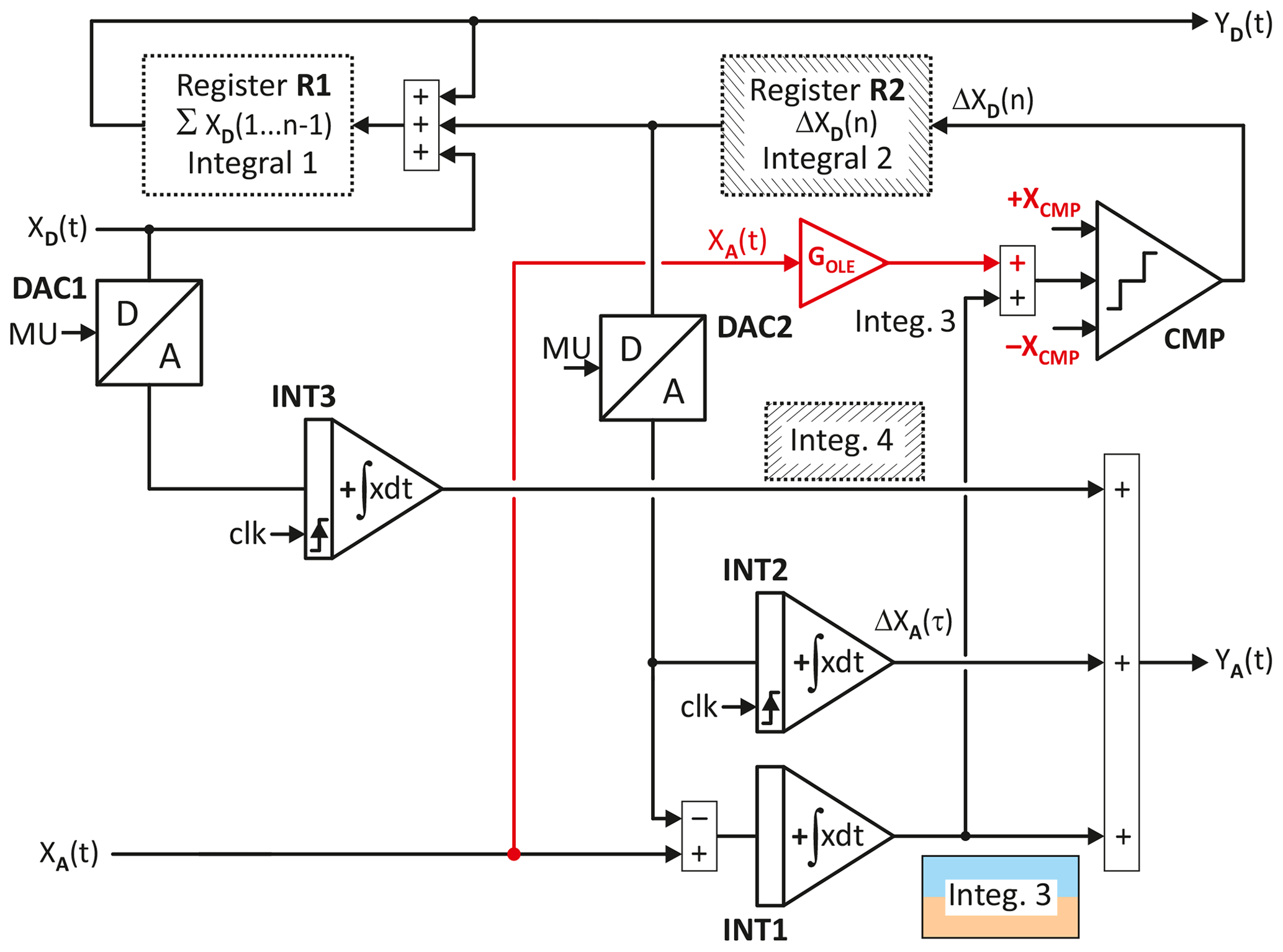
Figure 9New hybrid integrator with local feed back and predictive overload estimation of analog integrator.
In the following, we will demonstrate the operation of the hybrid integrator with local feedback using two classical examples, the harmonic oscillator and a damped spring-mass system. We then show a spiking neuron according to Hindmarsh and Rose (1984), which has significantly different time constants in the three differential equations and requires the scaling of at least one variable. Finally, we demonstrate the operation and advantages of the hybrid integrator with overload estimation using a second-order CT ΔΣ modulator. However, we do not perform detailed analyses of SNR or noise shaping, but take a look at the integrator states in the presence of step changes in the input signal at the limit of the dynamic range.
4.1 Harmonic oscillator on an analog computer
In this practical example the harmonic oscillator described by the differential equation is implemented. Figure 10 shows the Simulink model of such an oscillator, built from pure analog integrators.
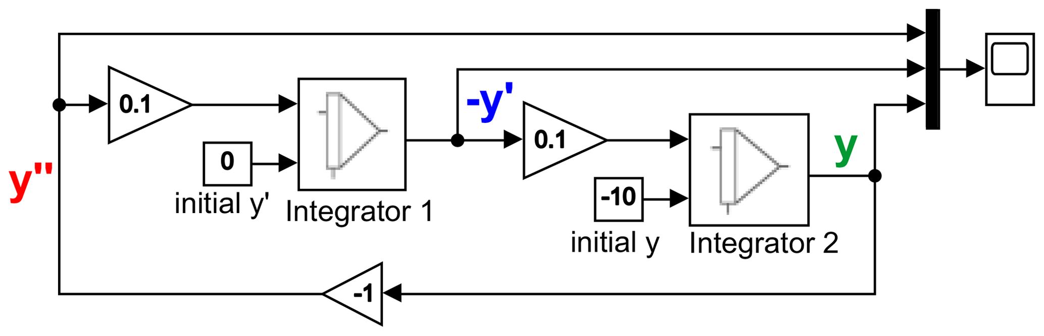
The analog computer circuit consists of integrators configured in a loop with coefficient elements ω=0.1 in between. A selection of signals from the harmonic oscillator simulation is shown in Fig. 11: The first diagram represents the signals YA+YD (y, in green color) composed of analog and digital parts, (y', in blue color), and (y”, in red color). In the middle and bottom diagrams of Fig. 11, the analog and digital portions of YA+YD (ya, in green color, yd, in light green color) and (y'a, in blue color, y'd, in light blue color) are shown.
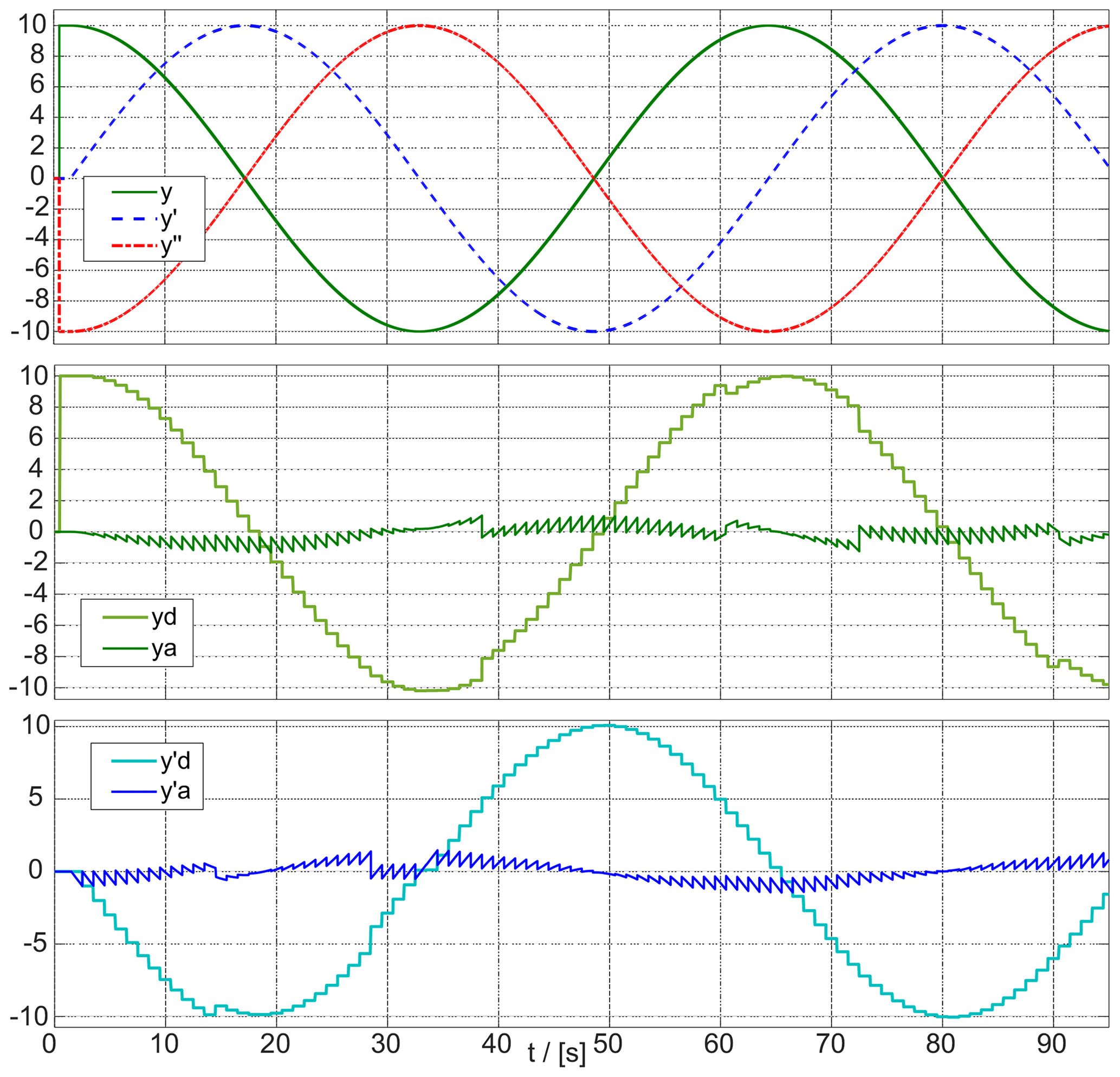
The initial condition is . This is realized by an initial digital value YD(0)=10, as can be seen in the middle of Fig. 11. Depending on how the digital LSBs are scaled with respect to the machine unit MU, not only multiples of the MU can be used as initial values in the hybrid integrator, but also fractions of a MU. Most of the amplitude is exchanged digitally between the integrators in the oscillator, as can be seen from the digital values YD and which reach full scale value 10. The analog parts YA and exceed MU only slightly up to approximately 1.5 MU, when YA+YD and have their zero crossings, i. e. when their derivative is at maximum amplitude. Crucial for this is that the digital slew rate of the Integral 1 is of the order of the slew rate of the total integral of the hybrid integrator.
4.2 Spring-mass-damper system on an analog computer
As a second example for the application of the hybrid integrator a damped spring-mass system is considered. The Simulink block diagram for this is shown in Fig. 12. At the top of the block diagram, a purely analog and continuous-time system is set up as a reference. The model corresponds to the unscaled model of Fig. 1, the result should correspond to the simulation result of Fig. 2.
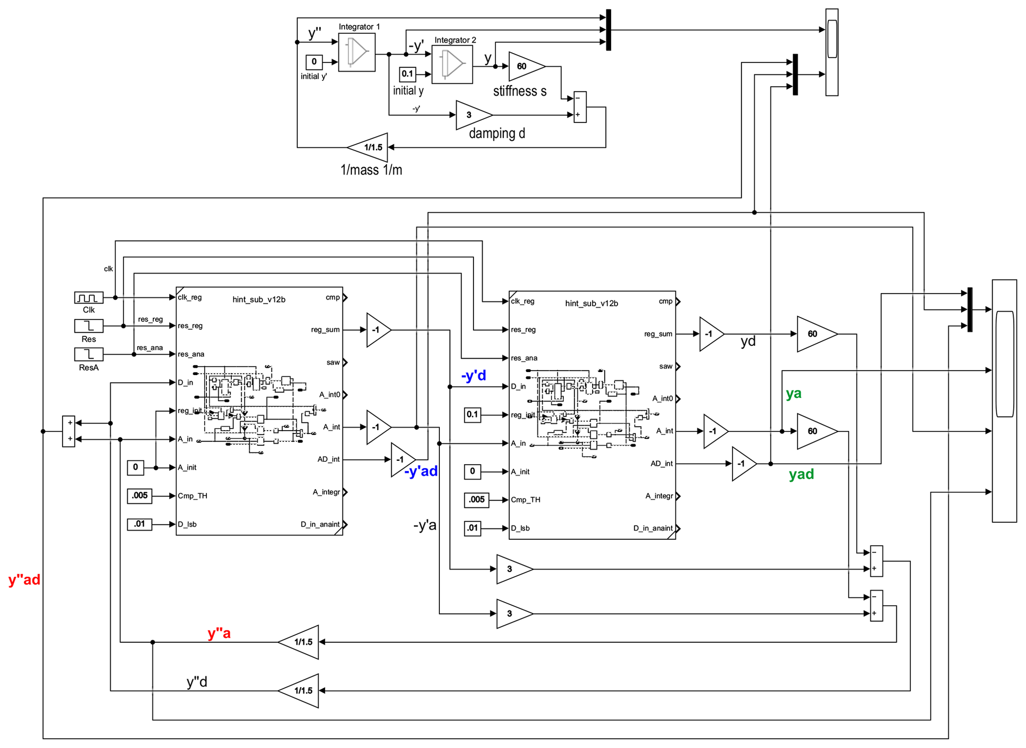
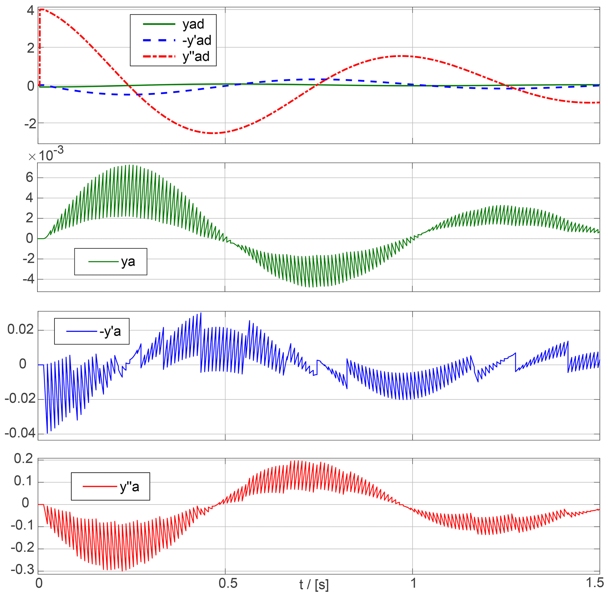
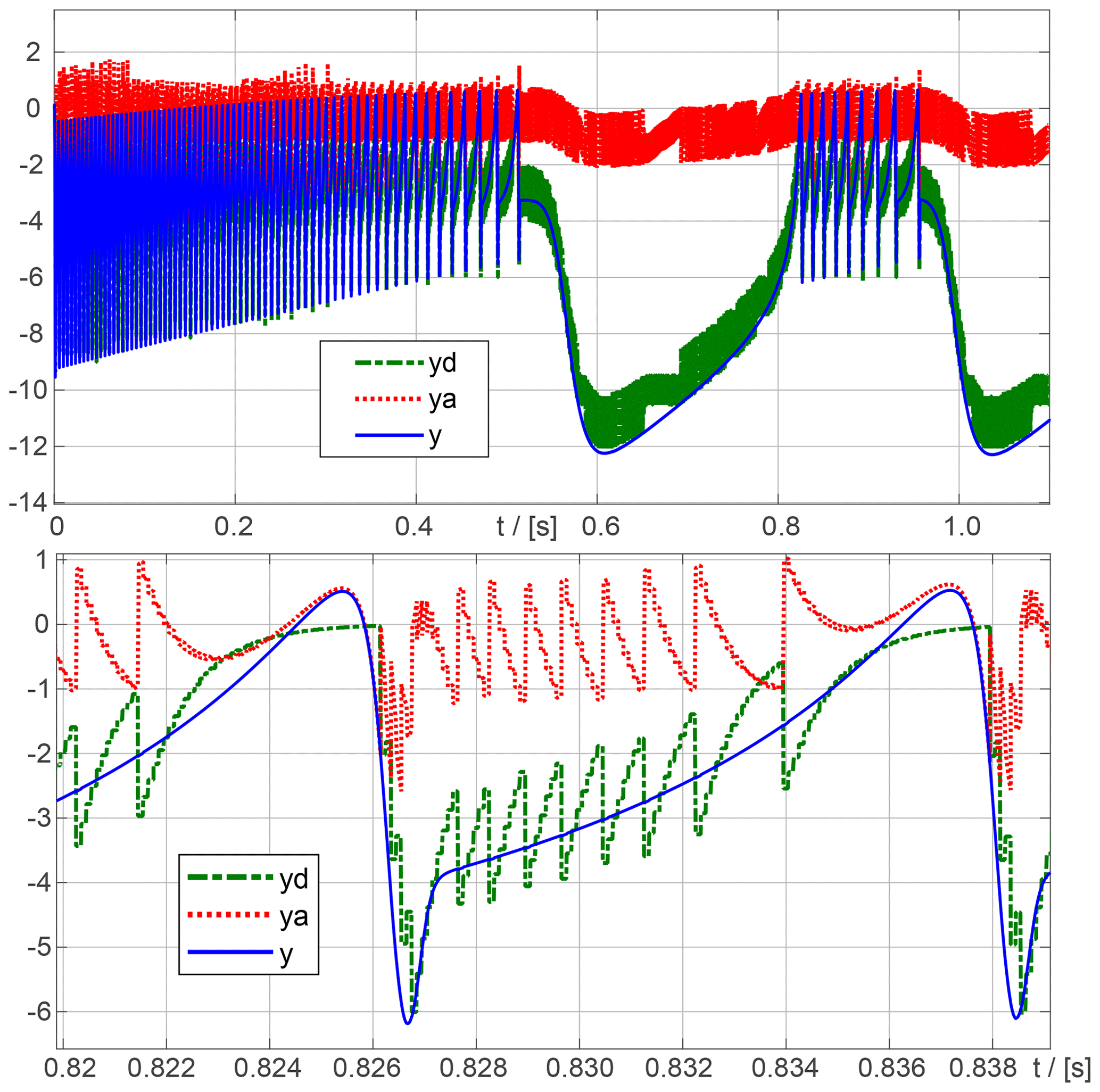
The integrators in the reference model are inverting. An initial value of 0.1 at the input of the second integrator thus leads to an initial displacement of −0.1. The Simulink module of the hybrid integrator is not inverting, so in Fig. 12 inverters are provided at the outputs reg_sum, A_int, and AD_int, respectively. reg_sum and A_int represent the analog and digital parts of the integral, respectively. At A_int the respective total integral is output after that the sign is changed and then output as yad (in green color), -y'ad (in blue color) and y”ad (in red color) shown in Fig. 13 above.
The period of the damped oscillation is about 1 s. For the digital part of the hybrid integrator to follow the signals, the clock frequency must be a multiple of the oscillation frequency. Therefore, the clock frequency was set to 100 Hz. To ensure that the digital portion of the integral has sufficient resolution, the equivalent analog value of a digital LSB was set to 0.01. The threshold value of the comparator is LSB. Since Register R1 (in Fig. 6) adds up the digital input XD(t) 100 times per second, digital integration requires scaling down the input XD(t) to the Register R1 by a factor of 100. If the Register R2 already contains the comparator value scaled down to the LSB, it must be scaled up again at DAC1 to generate the ramp signal ΔXA(τ) with slope 1 in integrator INT2.
In Fig. 13, in addition to the overall analog-digital quantities of the spring-mass-damper system, the respective analog portions ya (in green color), -y'a (in blue color) and y”a (in red color) are plotted. Since already y'a never exceeds 3 LSB, the pure analog fraction ya is never larger than 0.7 LSB, the (not shown) analog fraction Integral 3 representing ∫XA(t)dt is also only 0.2 LSB at most. With the chosen scaling with a small LSB and high clock frequency related to the oscillation frequency, no overflow from analog to digital takes place in the 2nd integrator.
The 1st integrator generates -y'a, having a maximum magnitude of 4 LSB. The fraction of Integral 3 of the first integrator is 0.5 LSB at most. Although -y'a exceeds 1 LSB this does not represent an overload: The peaks of the sawtooth-shaped waveform result from the high values at the digital input of the first integrator, which generate the periodic linear ramped integral component Integral 4 with the DAC1 and INT3. In practice, however, Integral 4 and Integral 3 are not added first, as shown in the block diagram. Instead, the summation is done with an adder circuit at the analog integrator in the subsequent second hybrid integrator.
In Fig. 13 y”a shows the largest values of all analog signals, which results from the factor 60 due to the spring constant. The analog input to the first integrator is therefore up to 30 LSB, resulting in overflows from analog to digital being generated in the first integrator, which can be seen from the steps in the sawtooth waveform of y'a.
The hybrid integrator enables simple interconnection of analog computing components without the need for scaling.
4.3 Spiking neuron
The third example is the implementation of a spiking neuron described by a set of differential equations on the analog computer. A well-known model here is that of Hindmarsh and Rose (1984), which consists of three coupled differential equations:
A bursting behavior as in Hindmarsh and Rose (1984) is obtained when a=1, b=3, c=1, d=5, , and the external current is set to I=2. Scaling the equations in time by multiplying the three derivatives , , and by a factor 1000, the neuron starts the first burst of pulses after 0.8 s simulation time, as shown in Fig. 14.
In the analog computer the integrator around y has a short time constant and simultaneously a large signal amplitude. Therefore the outputs of the integrators must be scaled down to the machine unit MU. For this purpose, x and z would be divided by 2, and y would be scaled down by a factor of 15.
An alternative to the extensive downscaling of y is the use of a hybrid integrator, as realized with the model in Fig. 15.

The three coupled differential equations require three integrators, integ_X, integ_Z, and integ_Y_hybrid. The hybrid integrator for y is operated at a clock rate of 10 kHz. The initial values for each of the three integrators are 0. The constant components are switched on after the start of the simulation and the initialization of the hybrid integrator after a clock period, i. e. after 100 µs.
The integrator for has direct feedback, as shown by Eq. (7). The feedback is also linear, so in contrast to the integrator for , it has no second or third powers in the feedback path. Therefore, it is possible to feed back the analog and digital components yd and ya separately to the analog and digital inputs of the hybrid integrator. In this case, only the clock frequency must be taken into account in the time scaling process. While the scaling factor 1000 is still used at the analog input ya' and thus the simulation is accelerated accordingly compared to the real time (wall clock), for the digital feedback at -yd the scaling factor 1000 has to be reduced to 0.1 because of the clock frequency of 10 kHz. Figure 16 shows in two diagrams respectively the curves of y, ya and yd.
To ensure that the analog overdrive, which is detected by the window comparator and thus increases the digital registers, is dominant over the negative digital feedback in any case, the digital LSB must be selected to be 2. As a result, a decrease of the analog ya can be limited to −2 on average, and even for transients to about −2.5 (lower figure in Fig. 16).
This example shows that when using hybrid integrators in analog computers it is not necessary to replace all integrators by hybrid integrators, instead this can be done according to the application. Furthermore, a local digital feedback can be implemented, but it must be ensured that a negative digital feedback does not prevent the carry over from analog to digital and thus the limiting of the output of the analog integrator. The digital part of the hybrid integrator can be converted from analog to digital by passing the individual bits of yd through weighted resistors to the summation input of integ_X.
4.4 CT ΔΣ modulator
In the last example, a hybrid integrator with predictive overload estimation (OLE) according to Fig. 9 was used to realize a CT ΔΣ modulator of second order without scaling. The modulator is constructed as in Fig. 3, only with 2 integrators. The coefficients are b1=1, a1=1 and b2=2. The b-coefficients are connected to the digital inputs XD(t) of the digital integrators. The hybrid integrators have a LSB=1, comparator thresholds of LSB, and a clock period T=1 s. The respective input XA(t) is weighted by a factor GOLE=0.5 for overload estimation and then added to the Integral 3. The clock of the quantizer is delayed by half a clock period, i. e. the registers and the comparator in the hybrid integrator operate on the rising clock edge, the quantizer on the falling clock edge.
In a Matlab-Simulink simulation bench, the time responses of the analog and digital components of the hybrid integrators are compared. The integrator with OLE according to Fig. 9 is compared with a version without OLE according to Fig. 6. We pay attention to how the hybrid integrators cope with overloads due to large input signals.
Both versions of the modulator, with and without OLE, of course give the same overall results, as shown by the bit stream v and the integrator outputs x1 and x2 in Fig. 17. The top plot in Fig. 17 also shows the input signal u increasing from 0.05 to 0.95 at t=5 s, triggering the overload.
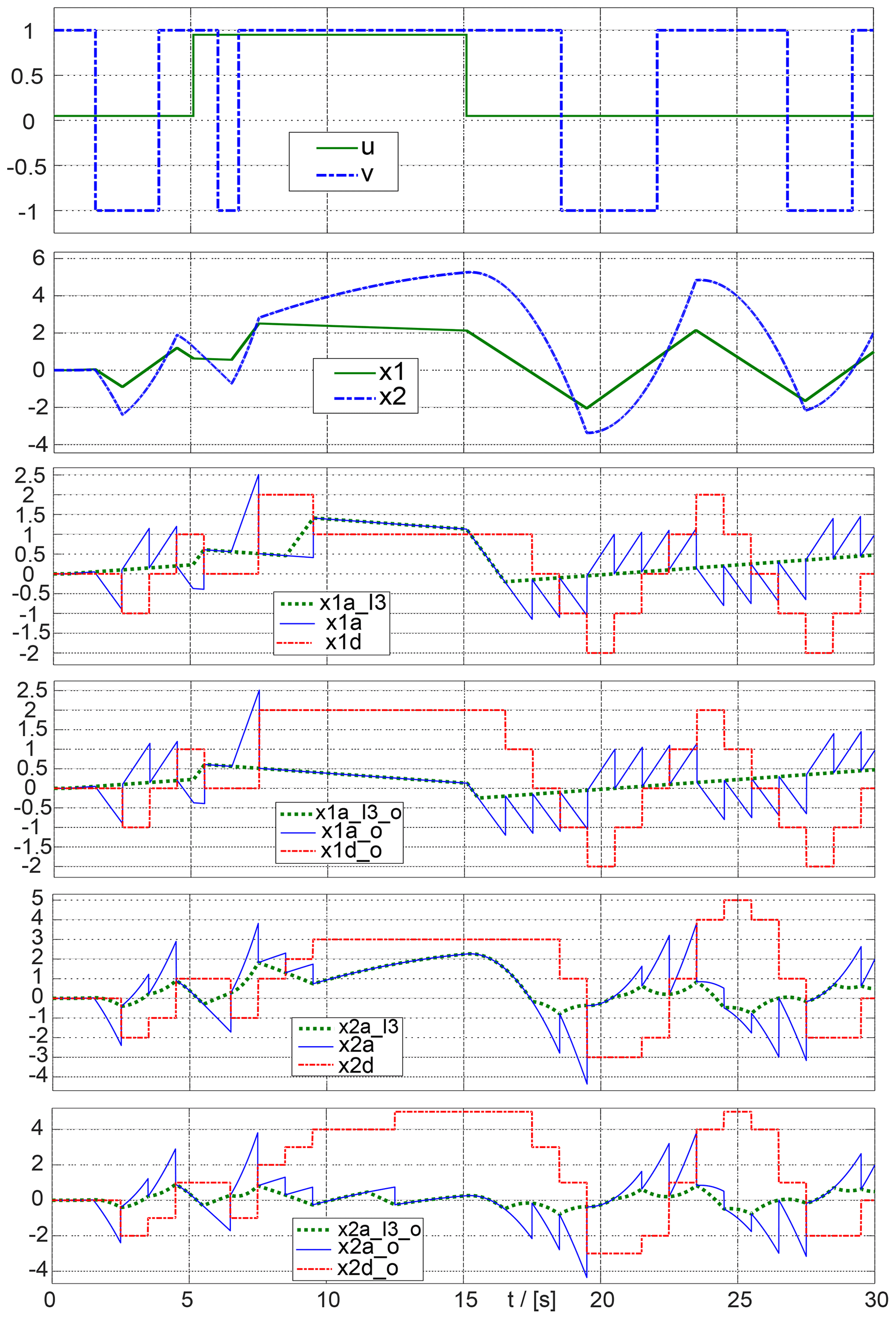
Figure 172nd order CT ΔΣ-Modulator under overload condition, using hybrid integrators, with and without overload estimation.
The two middle plots of Fig. 17 show the analog and digital components of the first integrator, the two lower plots those of the second integrator. Herein x1d, x2d, x1d_o and x2d_o are the digital parts, x1a, x2a, x1a_o and x2a_o the analog parts. Signal names ending with _o belong to the integrator with overload estimation. Signal names ending in …a_I3 are the respective parts of Integral 3, i. e. ∫XA(t)dt. As in section 4.2, it is necessary to distinguish between the analog sum signal YA(t)dt (denoted by x*a in Fig. 17) and the integral of the analog input ∫XA(t)dt. YA(t)dt can be represented by the instantaneous value of the contribution of XD(t) (Integral 4) and the contribution ΔXA(τ) being much larger than ∫XA(t)dt.
First, we compare the signal characteristics of the first integrator without overload estimation (OLE) with the one with OLE. The signal curves differ from t=8.5 s on. At t=8.5 s, Integral 3 (x1a_I3, dotted in green) falls below the threshold of 0.5, and the window comparator yields 0. The quantizer output v is positive, so at time t=9.5 s the digital component x1d is decremented by 1. Since at time t=8.5 s the window comparator output becomes 0, no continuous-time reset occurs, and x1a_I3 increases from 0.5 to just below 1.5 during a clock phase.
In contrast, for the hybrid integrator with OLE, the analog input u=0.95 is multiplied by GOLE=0.5 even after t=8.5 s and added to Integral 3, the comparator threshold continues to be exceeded, and the Integral 3 continues to be subjected to a continuous-time reset until t=15.5 s. Overload estimation keeps the analog Integral 3 below the threshold of 0.5.
The advantages of OLE are also evident in the second integrator: At t=6.5 s, Integral 3 is just above the zero line, the window comparator in the hybrid integrator without OLE yields 0, so that at t=7.5 s x2a_I3 increases to 2. In the integrator with OLE, the window comparator output is positive, so that at t=7.5 s x2a_I3_o is still below 1. At t=11.5 s, similar behavior can be seen: By OLE, the comparator is positive, the x2a_I3_o is reduced by time t=12.5 s, and the digital part of the integral x2d_o reaches 4.
Due to the OLE, the analog integral of the 1st integrator can always be kept below 1 MU. Despite the peak values for the analog sum signal x1a_o for the first integrator, the analog Integral 3 (x2a_I3_o) of the second integrator is also kept under 1 MU.
At the output of the second integrator, the sum signal x2a_o and the digital output x2d_o must be evaluated together in the quantizer, which typically requires a suitable DA conversion of the digital value.
The new improved hybrid integrator with overload estimation is well suited for applications without negative feedback and for signals with steep transients and can therefore be used universally in analog computers, CT ΔΣ modulators, and analog control circuits.
A significant feature is that the digital component stored in the hybrid integrator does not have to be converted into an analog sawtooth voltage and fed to the analog output. Only the overflow of one bit corresponding to a machine unit (MU) that occurred in the hybrid integrator must be taken into account during a clock phase in the analog part, as well as the digital input to the hybrid integrator, of course. The reset of the analog component of the hybrid integrator is done continuously in time. During the reset process, an additive ramp signal is used to achieve a continuously correct value for the analog part of the hybrid integral. After the reset process, the ramp signal is switched off and the digital component is incremented. Disadvantages due to capacitive resets are thus avoided. Also, disadvantages due to asynchronous digital counters and the need for high-precision continuous-time comparators can be avoided in integration methods with integration direction reversal.
Due to the synchronous operation it is possible to use precisely clocked regenerative comparators, and because of the continuous-time reset a a precise representation of the total integral is possible. In contrast to this, of course, the overall circuit complexity must also be taken into account. In particular, this is relevant if the digital part of the analog integral has to be further processed in the analog computer, and thus the circuitry overhead and errors in the DA conversion have to be taken into account.
For overload estimation, the current analog input is added to the analog part of the integral with a weighting factor, so that in the case of dynamically changing signals or transients, the maximum magnitude of the analog integrator can be safely kept below one machine unit MU. However, the effectiveness of the overload estimation also depends on the specific signal waveform.
Through simulations of a harmonic oscillator, a damped spring-mass system, a spiking Neuron, and a CT ΔΣ modulator, it has been shown that scaling from the mathematical model to the real circuit with limited voltages is simplified, and the dynamic range can be extended almost arbitrarily by the hybrid representation of the integral.
The Matlab models may be obtained by the authors and are subject to confidentiality.
No data sets were used in this article.
DK developed the Matlab models. BU and SK contributed with applications, and contributed to review and editing this article.
At least one of the (co-)authors is a member of the editorial board of Advances in Radio Science. The peer-review process was guided by an independent editor, and the authors also have no other competing interests to declare.
Publisher’s note: Copernicus Publications remains neutral with regard to jurisdictional claims in published maps and institutional affiliations.
This article is part of the special issue “Kleinheubacher Berichte 2022”. It is a result of the Kleinheubacher Tagung 2022, Miltenberg, Germany, 27–29 September 2022.
This paper was edited by Jens Anders and reviewed by two anonymous referees.
Au, S. and Leung, B. H.: A 1.95-V, 0.34-mW, 12-b sigma-delta modulator stabilized by local feedback loops, IEEE J. Solid-St. Circ., 32, 321–328, https://doi.org/10.1109/4.557629, 1997. a
Bryant, M. D., Yan, S., Tsang, R., Fernandez, B., and Kumar, K. K.: A Mixed Signal (Analog-Digital) Integrator Design, IEEE T. Circuits I, 59, 1409–1417, https://doi.org/10.1109/TCSI.2011.2177133, 2012. a, b, c
Hall, C. R. and Kahne, S. J.: An improved method for analog computer scaling, Math. Comput. Simulat., 12, 27–32, https://doi.org/10.1016/S0378-4754(70)80022-2, 1970. a
Hindmarsh, J. L. and Rose, R. M.: A model of neuronal bursting using three coupled first order differential equations, P. Roy. Soc. Lond. B, 221, 87–102, https://doi.org/10.1098/rspb.1984.0024, 1984. a, b, c
Howe, R. M.: Fundamentals of the analog computer: circuits, technology, and simulation, IEEE Control Systems, 25, 29–36, https://doi.org/10.1109/MCS.2005.1432596, 2005. a
Jin, X.-Z., Che, W.-W., Wu, Z.-G., and Wang, H.: Analog Control Circuit Designs for a Class of Continuous-Time Adaptive Fault-Tolerant Control Systems, IEEE T. Cybernetics, 52, 4209–4220, https://doi.org/10.1109/TCYB.2020.3024913, 2022. a
Killat, D., Ulmann, B., and Köppel, S.: Hybrid integrators for analog computers, in: 2022 Kleinheubach Conference, 27–29 September 2022, Miltenberg, Germany, 1–4, ISBN 978-3-948571-07-8, 2022. a
Navarro, S. O.: Analog Computer Fundamentals: With an Introduction to Matrix Programming Methods, University of Michigan, 1962. a
O'Grady, E. P.: A hybrid-code differential analyzer, Math. Comput. Simulat., 8, 13–21, https://doi.org/10.1016/S0378-4754(66)80044-7, 1966. a, b, c
Ortmanns, M. and Gerfers, F.: Continuous-time sigma-delta A/D conversion: Fundamentals, performance limits and robust implementations, vol. 21 of Springer series in advanced microelectronics, Springer, Berlin and New York, https://doi.org/10.1007/3-540-28473-7, 2006. a, b
Shim, J. H., Park, I.-C., and Kim, B.: Hybrid ΣΔ modulators with adaptive calibration, IEEE T. Circuit. Syst. I, 52, 885–893, https://doi.org/10.1109/TCSI.2005.846229, 2005a. a, b
Shim, J. H., Park, I.-C., and Kim, B.: A third-order ΣΔ modulator in 0.18µm CMOS with calibrated mixed-mode integrators, IEEE J. Solid-St. Circ., 40, 918–925, https://doi.org/10.1109/JSSC.2005.845558, 2005b. a
Skramstad, H. K.: A combined analog-digital differential analyzer, in: Papers presented at the December 1–3, 1959, eastern joint IRE-AIEE-ACM computer conference on – IRE-AIEE-ACM '59 (Eastern), edited by: Heart, F. E., 94–100, ACM Press, New York, New York, USA, https://doi.org/10.1145/1460299.1460309, 1959. a, b, c, d, e, f, g
Tsividis, Y. and Guo, N.: Systems and methods for preventing saturation of analog integrator output, US9171189B2, 2015. a
Ulmann, B.: Analog Computing: Chap. 7.5 – Scaling, De Gruyter Textbook, De Gruyter Oldenbourg, München and Wien, 2nd extended edn., https://doi.org/10.1515/9783110787740, 2022. a
Ulmann, B., Köppel, S., and Killat, D.: Open Hardware Analog Computer for Education – Design and Application, in: 2021 Kleinheubach Conference, 28–30 September 2021, Miltenberg, Germany, 1–2, https://doi.org/10.23919/IEEECONF54431.2021.9598447, 2021. a
Wait, J. V.: A HYBRID ANALOG-DIGITAL DIFFERENTIAL ANALYZER SYSTEM, PhD Thesis, University of Arizone, https://repository.arizona.edu/bitstream/10150/284501/1/azu_td_6404038_sip1_m.pdf (last access: 14 August 2023), 1963. a, b, c