 | 19 Sep 2019
A low complexity digital frequency calibration with high jitter immunity for ultra-low-power oscillators
Markus Scholl
Ralf Wunderlich
Stefan Heinen
This paper presents a highly efficient digital frequency calibration method for ultra-low-power oscillators in wireless communication systems. This calibration method locks the ultra-low-power oscillator's output frequency to the reference clock of the wireless transceiver during its send- and receive-state to achieve frequency stability over process variation and temperature drifts. The introduced calibration scheme offers high jitter immunity and short locking periods overcoming frequency calibration errors for typical ultra-low-power oscillator's by utilizing non-linear segmented feedback levels. In measurements the proposed calibration method improves the frequency stability of an ultra-low-power 32 kHz oscillator from 53 to 10 ppm ∘C−1 over a wide temperature range for temperature drifts of less than 1 ∘C s−1 with an estimated power consumption of 185 nW while coping with relocking periods of 7 ms.
- Article
(6328 KB) - Full-text XML
- BibTeX
- EndNote


The demand for low power RF communication architectures in today's rapidly growing markets as the internet of things (IoT), smart utility networks (SUN), wireless sensor networks (WSN) and cyber-physical systems (CPS) has increased to support long battery lifetime on a stringent energy budget. These architectures utilize an advanced duty-cycle scheme either based on wake-up timer for a time slot based communication protocol (TDMA) or on wake-up receiver to reduce power consumption on system level. Both architecture types require a stable ultra low power (ULP) low frequency clock source with absolute frequency accuracy to implement a reliable and power saving duty cycle scheme in TDMA systems or for precise baseband data sampling in a wake-up receiver as discussed by Burdett (2015).
In prior works, several efforts have been made to achieve absolute frequency accuracy over process variation and temperature drifts.
However, the conventional approach of using an external low frequency crystal (XTAL) as demonstrated by Yoon et al. (2016) increases the external component count and therefore increases the total cost of the wireless communication system. Other approaches proposed by Paidimarri et al. (2013) and Griffith et al. (2014) achieve absolute frequency accuracy by costly factory calibration and also require high temperature stability of the used ULP oscillator leading to increased power consumption in the oscillator design. More application tailored solutions utilize existing clock signals in a complex system with absolute frequency accuracy but different frequency and design requirements as a reference for an on-chip calibration method. Shrivastava and Calhoun (2012) propose a periodic recalibration scheme based on an existing clock signal to achieve absolute frequency accuracy and compensate frequency drifts over temperature changes relaxing the design requirements of the ULP oscillator's temperature stability leading to potentially lower power consumption and lower area. Nonetheless, this calibration technique uses a successive approximation algorithm which typically have high jitter sensitivity degrading the frequency calibration accuracy. These on-chip calibration methods like FIR-filter based calibration loops suffer from contradictory requirements of low bandwidth of the loop to suppress jitter resulting in high settling time and the calibration accuracy degradation by increased noise.
This work presents a calibration technique overcoming the contradictory requirements of high jitter immunity to guarantee the optimum calibration word and fast settling time by using multi-level bang-bang algorithm. This technique has been used in Scholl et al. (2016) to dramatically increase the performance and especially the temperature stability of an ULP oscillator. The non-linear segmentation of the calibration error in the feedback path allows a large feedback gain for large frequency error leading to a fast settling but also has a very small feedback gain once the frequency tuning word has settled to achieve high jitter tolerance. For a faster relocking in active states of the TRX the calibration algorithm is synchronized to the ULP oscillator to reduce the error signal in the first calibration cycle of the relocking to a minimum. The low complexity of the proposed calibration technique leads to an efficient digital implementation with low power consumption.
In Fig. 1 a block diagram of a simplified wireless transceiver (TRX) is depicted. The frequency synthesizer (PLL) is used to generate a local oscillator (LO) signal to down convert the received RF signal to the baseband which is filtered and digitized for further signal processing and demodulation. Additionally, the PLL is used to generate a modulated RF signal which is amplified and fed to the antenna during transmit state. To meet the strict requirements for absolute frequency accuracy of the transmitted signal and also for the LO signal, resulting from the dense channel allocation in the limited RF band, a precise crystal oscillator is used in every TRX as an absolute frequency reference. This oscillator's frequency depends on the exact application and communication standard but is typically in a range between 10 and 50 MHz.
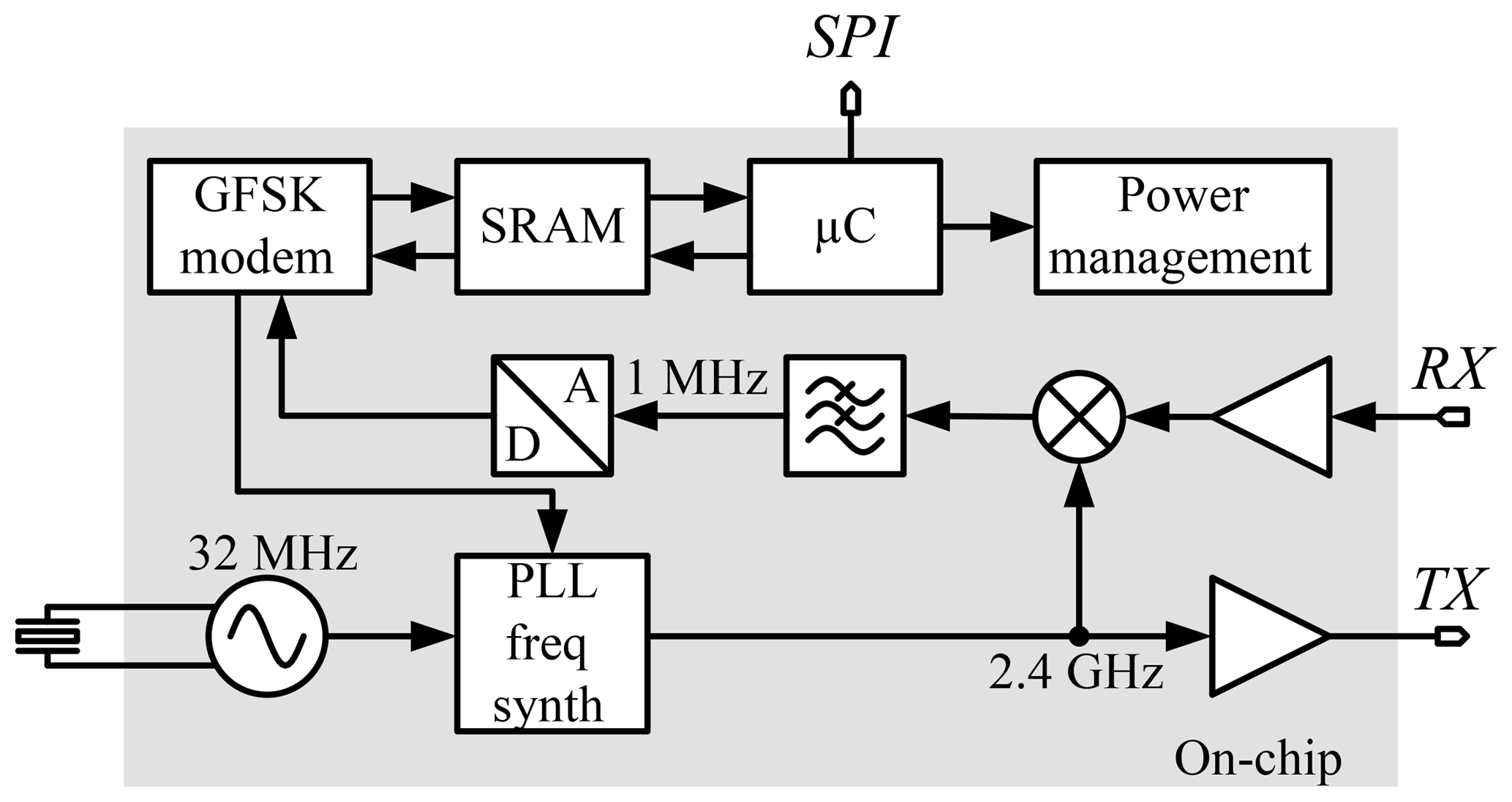
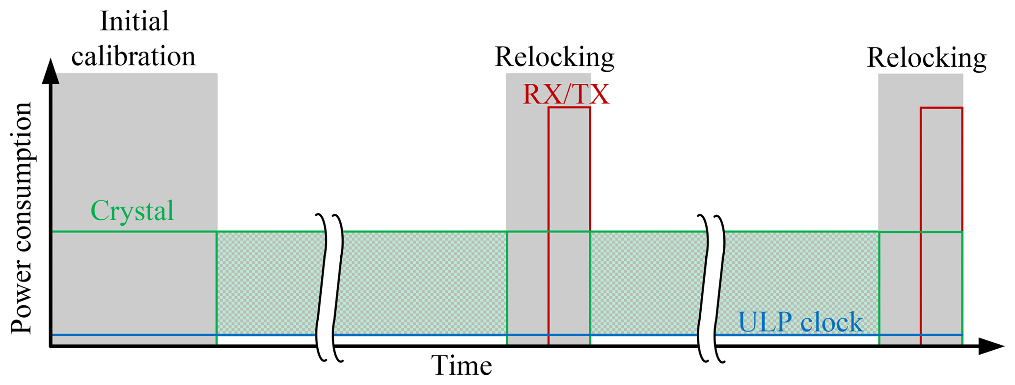
Since many of these wireless TRX are used in devices which are battery operated there is a high demand to reduce average power consumption of the TRX to extend lifetime of the devices. Therefore, advanced duty cycle schemes have been implemented for TDMA protocols exploiting the deterministic timeslot for transmit and receive operation and powering down most circuits of the TRX in between. In these systems it is critical to determine the time point before the next dedicated timeslot to turn-on all necessary circuits. This determination is realized with a wake-up timer counting clock cycles of either the main crystal oscillator or of a dedicated ULP oscillator typically in the range of 32 and 64 kHz. This low frequency ULP oscillator is implemented to measure a timespan with a certain required accuracy while having much lower power consumption compared to the crystal oscillator. Thus the main crystal oscillator is only active during the send- and receive-state of the TRX if a dedicated ULP oscillator is implemented and the power consumption can be further reduced as visualized in Fig. 2. In this phases the main crystal oscillator can also be used as reference frequency to calibrate the ULP oscillator to overcome frequency deviations due to process variation. The red curve indicates the power consumption of all blocks necessary to receive or transmit data as these are only active during the dedicated time slots. The green curve gives the power consumption of the crystal oscillator while the blue curve represents the power consumption of the ULP oscillator. In light green the area representing the energy which can be saved by implementing an ULP oscillator is visualized.
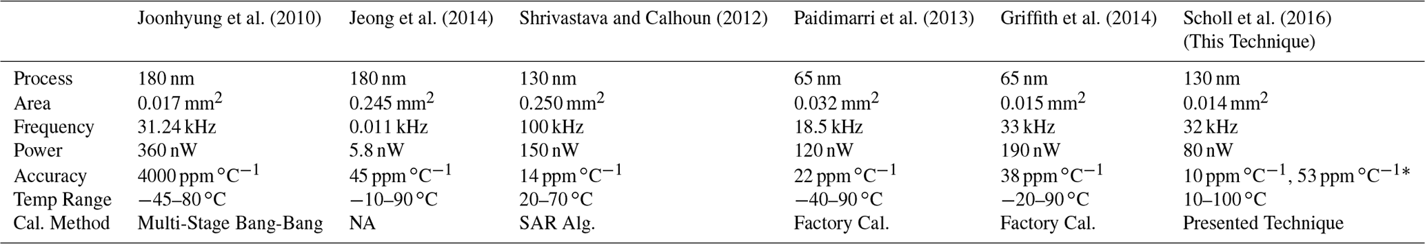
In Table 1 different implementation approaches as analyzed by Franklin et al. (2014) for frequency calibration loops are compared for the most relevant performance characteristics in this application as design complexity, area demand, power consumption and a performance indication for the tradeoff between frequency accuracy and settling time.
Analog filter based frequency calibration loops offer low power consumption due to the full custom transistor level design flow but also suffer from the complexity and various design choices of this design flow. This designs and especially the low frequency analog filter, necessary to suppress the high jitter of the clock signal to achieve high frequency accuracy, demand for large area. Furthermore, it is challenging to apply very low duty-cycling ratios resulting from the short locking periods in which the reference clock is available to this calibration loop due to the analog output voltage drift caused by leakage currents.

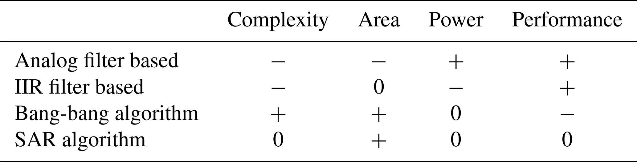
IIR filter based frequency calibration loops overcome these output voltage drift issues because digital circuits and digital signal representation are inherently tolerant to leakage current. The downside of this calibration approach are the digital multiplications needed in the IIR filter resulting in high power consumption.
The bang-bang algorithm is based on a very simple principle as it increases the digital tuning word by a fixed step size if the frequency of the ULP oscillator is too high and decreases the tuning word by the same amount if the output frequency is too low. Due to its simplicity this calibration approach can be implemented with high power and area efficiency. On the other hand the fixed step size leads to an unfavorable tradeoff between settling time, calibration accuracy and jitter immunity making this approach not suitable for applications with low duty-cycle ratios.
Frequency calibration with a SAR algorithm can also be implemented very area and power efficient because it is using binary decisions based on the sign of the frequency deviation and there are no calculations with the actual frequency deviation word. Additionally, the utilized binary search approach, which can also be seen as an inverse binary weighted step size, leads to a fast settling of this calibration approach. A critical drawback of this approach is the missing relocking capability leading to a full calibration cycle in every relocking period independent from the actual frequency deviation. Even more critical are the facts that the SAR logic is very prone to jitter because the step size is not adapted to the current frequency error and an error at the beginning of the calibration cycle cannot be corrected in later steps heavily degrading the calibration accuracy. Fig. 3 illustrates a calibration cycle of a SAR logic for an oscillator with high jitter and it also demonstrates how the jitter affects the calibration accuracy. The upper graph shows the output tuning word of the SAR logic controlling the frequency of an oscillator whereas the lower graph gives the actual clock signal of the oscillator in the black curve, the desired period length in red arrows, a Gaussian distributed jitter probability in blue and the clock signal with jitter as a green edge within the circle. In the first two calibration steps the algorithm performs as expected by testing if the oscillator's frequency is too high or low compared to the desired value for the tuning word “100000” and “010000”. In the third step the frequency tuning word is set to “011000” and the frequency is measured to be high because the ULP oscillator's clock edge occurs earlier due to jitter. Therefore the third bit is falsely detected as a “1” and consequently all following bits will be detected as “0” because the oscillator's output frequency is too low.
To overcome the limitations of the SAR and bang-bang algorithm but also avoiding the power consumption of the IIR filter based calibration a multi-level bang-bang algorithm as shown in Fig. 4 is presented in this work. The non-linear segmentation allows a large feedback gain for large frequency error leading to a fast settling but also has a very small feedback gain once the frequency tuning word has settled to achieve high jitter tolerance.
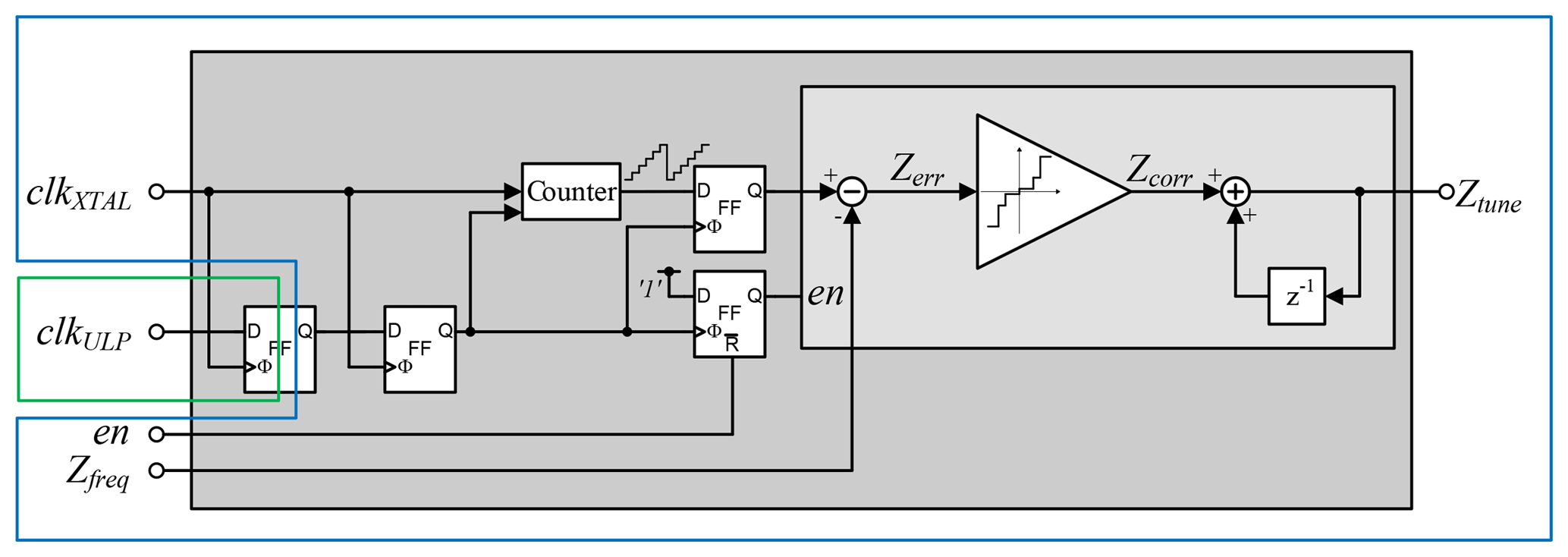
The frequency error Zerr is calculated from the ULP oscillator's clock and the reference clock from the crystal oscillator of the wireless transceiver by a frequency detector consisting of a counter, a register and a digital subtraction. The counter is clocked with the reference clock and its value is stored in a flip-flop at the synchronized rising edge of the ULP oscillator's clock signal. To fasten the relocking during active state of the reference clock signal the counter's restart bit is synchronized to the ULP oscillator's clock signal minimizing the first calculated error value of each relocking cycle. The frequency error Zerr is calculated from the stored counter value by subtraction a constant word Zfreq, determining the frequency ratio between the ULP clock and the reference clock. Afterwards this error signal is non-linearly segmented into three different levels representing a correction word Zcorr. This correction word is added to the tuning word Ztune as the output of the calibration logic. By choosing the segmentation levels as given in Eq. (1) the segmentation can be very efficiently implemented in digital logic.
To achieve optimal performance the smallest level covers all errors Zerr caused by jitter of the ULP oscillator after settling of the calibration loop to ensure the smallest feedback gain with highest calibration accuracy. This error range can be estimated from the 3σ-range of the rms-jitter of the oscillator. Additionally, errors resulting from non-linearities or changing of the feedback gain are avoided by this choice of range because only the smallest level occurs after settling. The larger segmentation levels represent a trade-off between stability of the feedback loop and settling time of the calibration.
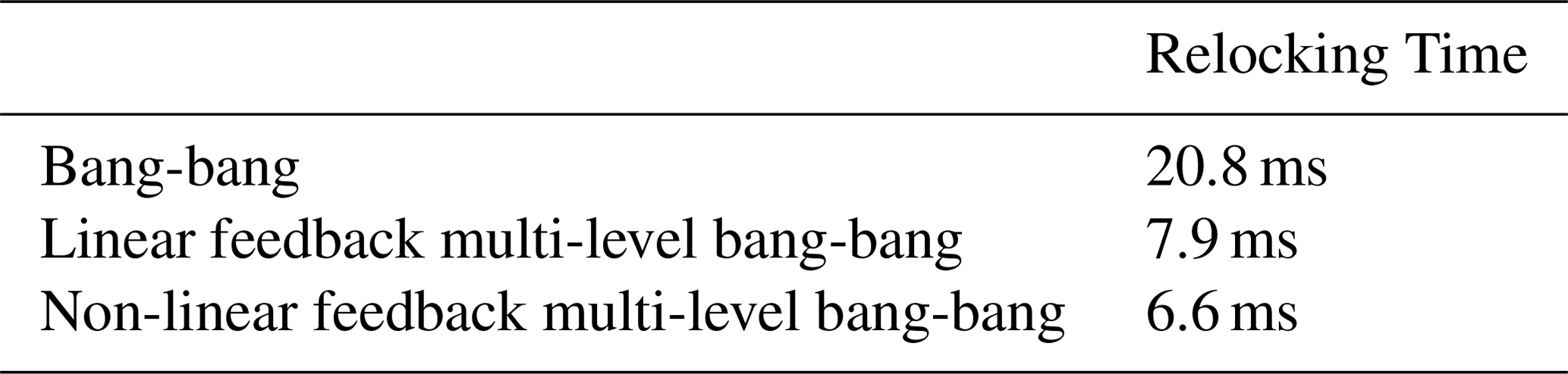
To further validate the choice of error range and segmentation levels simulation results for the relocking time of different bang-bang algorithm implementations are given in Table 2. In simulation a standard bang-bang calibration loop using only the smallest segmentation level of the other implementations achieving 20.8 ms relocking time is compared to two different multi-level bang-bang calibration loops. One of these multi-level loops uses a linear segmented feedback path resulting in 7.9 ms relocking time and the other one uses a non-linear segmentation as implemented in the presented design achieving 6.6 ms relocking time.
Table 2Comparison of different bang-bang algorithm implementations.
To avoid problems related to clock domain crossing the ULP oscillator's clock signal is synchronized to the reference clock domain by a two flip-flop synchronizer avoiding metastability of this signal. Besides this synchronization all other signals, registers and computations are in the clock domain of the reference clock avoiding problems with clock domain crossing in this design.
Joonhyung et al. (2010)Jeong et al. (2014)Shrivastava and Calhoun (2012)Paidimarri et al. (2013)Griffith et al. (2014)Scholl et al. (2016)Table 3Performance comparison of ULP oscillators with different calibration approaches.
* Without periodic relocking. NA: not available.
The presented digital frequency calibration method has been designed and evaluated using synthesized hardware description language on an Virtex-5 FPGA platform. For measurements the FPGA is connected to a custom designed ULP low frequency digitally controlled oscillator (DCO) on a separate ASIC fabricated in a 130 nm technology which was presented by Scholl et al. (2016). The ULP oscillator's clock signal and a 32 MHz reference clock signal are connected to the FPGA while the 9 bit frequency tuning word from the calibration loop is written from the FPGA to the custom ASIC with a 8 MHz SPI interface. The latency caused by communication over a SPI interface instead of parallel wired connection to the analog circuitry is neglectable in the measurement.
Additional synthesis results for a co-integrated on-chip implementation of the presented digital frequency calibration in the 130 nm technology estimate a power consumption of 26.4 µW during relocking and 5120 µm2 occupied area. The estimated power consumption during relocking Pcal translates to an average power consumption Pavg of
for a periodic 7 ms relocking cycle every second.
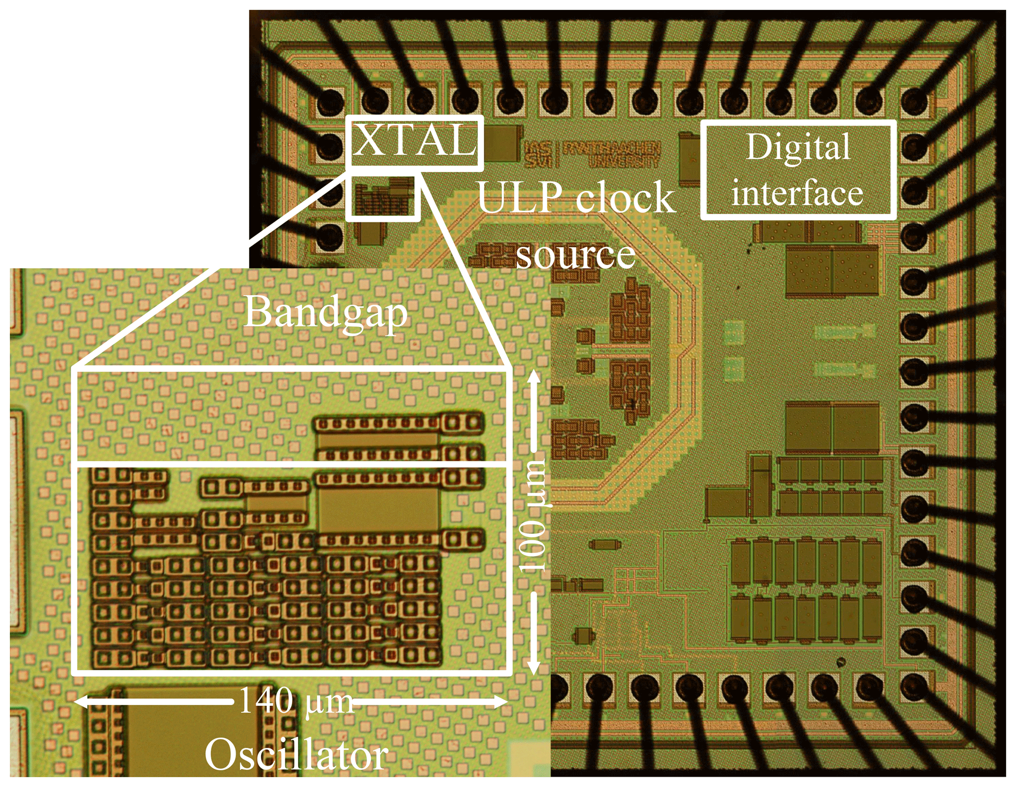
A micrograph of the 32 kHz ULP DCO used in measurement is shown in Fig. 5, occupying 100 µm×140 µm area. The power consumption of this ULP oscillator is 80 nW from a 1.2 V supply voltage. This design has a measured rms-jitter of 1.0 µs resulting from the current-source-based oscillator topology demanding for high jitter immunity of the digital frequency calibration method.
Figure 6 shows a measured calibration cycle with initial locking and relocking after a provoked frequency error demonstrating fast relocking capability and high jitter immunity. The blue curve illustrates the output Ztune of the digital frequency calibration loop whereas the red curve represents the Zerr signal in the digital logic indicating the current frequency error. During the 20 ms initial calibration phase different feedback levels can be observed as the slope of the frequency tuning word changes. After provoking a small frequency error the digital calibration loop relocks the oscillator's output frequency within 7 ms.
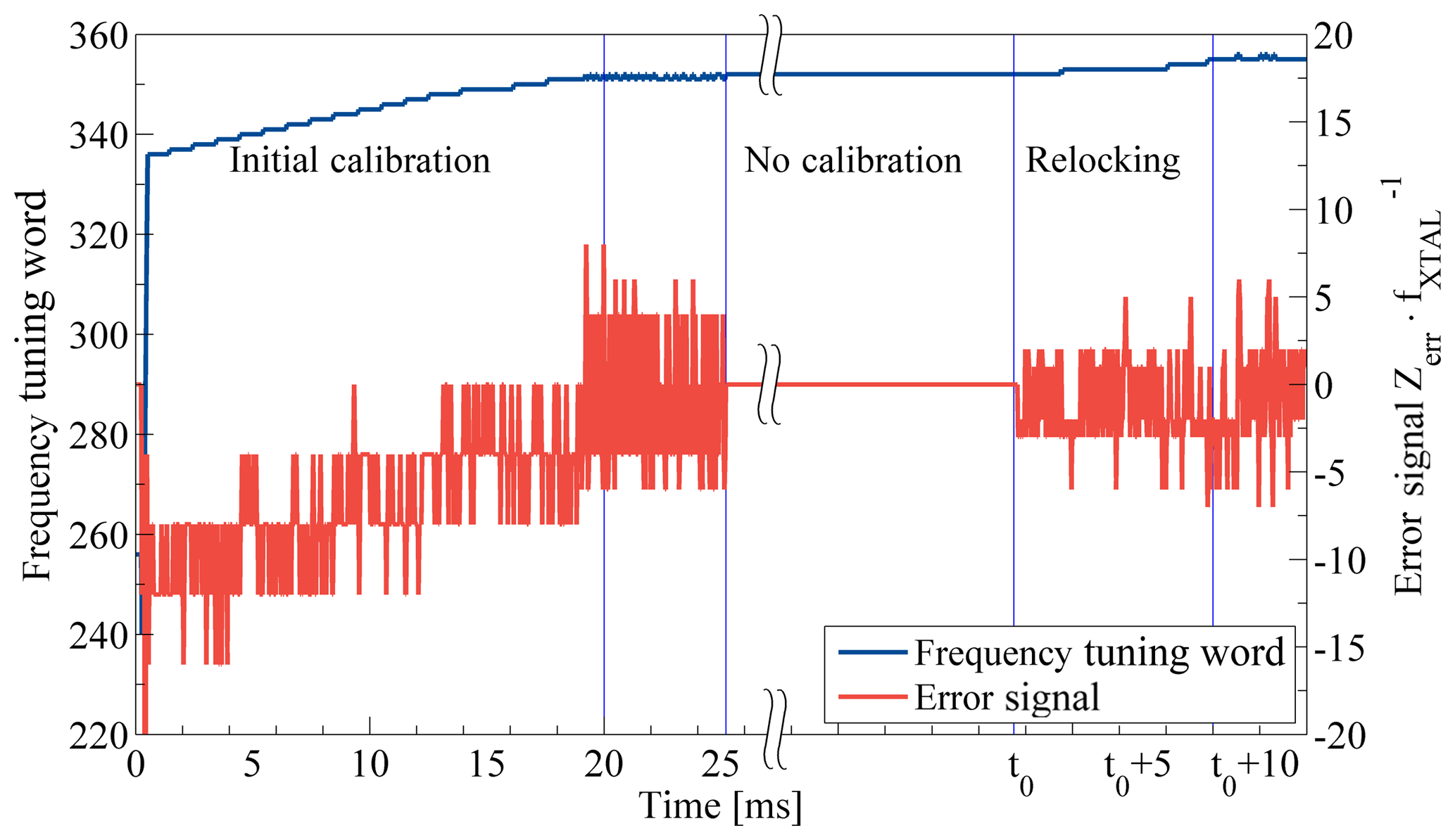
Figure 6Measured calibration cycle with initial locking and relocking after provoked frequency error.
In Fig. 7 the measured output frequency of the ULP oscillator over a temperature range from 10 to 100 ∘C and temperature gradients of 1 ∘C s−1 is shown. The blue line represents the measured oscillator's output frequency with an initial calibration cycle whereas the red dash-dotted line shows the output frequency after periodic relocking every second. The presented periodic relocking calibration scheme improves the ULP oscillator's frequency stability over temperature from 53 to 10 ppm ∘C−1.
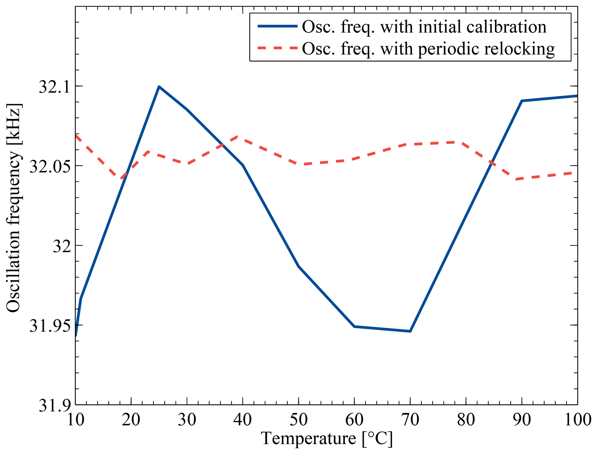
Figure 7Measured improvement in the temperature stability of the ULP oscillator's frequency with initial calibration and periodic recalibration for small temperature gradients of 1 ∘C s−1.
Table 3 gives a comparison between other published works and the ULP low frequency clock generation from Scholl et al. (2016) utilizing the proposed and analyzed frequency calibration method to improve the system performance. With the frequency calibration method discussed in this work the previous published clock generation system improves the temperature stability of the oscillator from 53 to 10 ppm ∘C−1 and therefore exhibit the temperature stability of other published works for similar temperature ranges with lower power consumption.
A highly efficient, low effort digital frequency calibration method with high jitter immunity specially tailored to ultra-low-power oscillators in wireless communication systems has been presented. By overcoming typical issue of ULP oscillators and enabling fast relocking with a non-linear segmented feedback in the calibration loop, the temperature stability of a custom designed ULP oscillator has been improved from 53 to 10 ppm ∘C−1 for small temperature gradients of 1 ∘C s−1 and periodic relocking after 1 s. Measurements validate the design choices and demonstrate fast and precise settling for ULP oscillators with high jitter output signals while maintaining low power consumption and area. Due to its simplicity and flexibility, it can be added as a straight-forward temperature stability enhancement technique for ULP clock sources in wireless communication systems.
The data are available upon request.
The authors declare that they have no conflict of interest.
This article is part of the special issue “Kleinheubacher Berichte 2018”. It is a result of the Kleinheubacher Tagung 2018, Miltenberg, Germany, 24–26 September 2018.
This paper was edited by Jens Anders and reviewed by two anonymous referees.
Burdett, A.: Ultra-Low-Power Wireless Systems: Energy-Efficient Radios for the Internet of Things, in: IEEE Solid-State Circuits Mag., 18–28, https://doi.org/10.1109/MSSC.2015.2417095, 2015. a
Franklin, G. F., Powell, J. D., and Emami-Naeini, A.: Feedback Control of Dynamic Systems 7th, Prentice Hall Press Upper Saddle River, NJ, USA, 2014. a
Griffith, D., Røine, P. T., Murdock, J., and Smith, R.: A 190 nW 33 kHz RC oscillator with ±0.21 % temperature stability and 4 ppm long-term stability, in: Int. Solid-State Circuits Conf. Dig. Tech. Papers (ISSCC), 300–301, https://doi.org/10.1109/ISSCC.2014.6757443, 2014. a, b
Jeong, S., Lee, I., Blaauw, D., and Sylvester, D.: A 5.8 nW, 45 ppm/∘C on-chip CMOS wake-up timer using a constant charge subtraction scheme, in: Proc. Custom Integrated Circuits Conf. (CICC), 1–4, https://doi.org/10.1109/CICC.2014.6946008, 2014. a
Joonhyung, L., Kwangmook, L., and Koonsik, C.: Ultra low power RC oscillator for system wake-up using highly precise auto-calibration technique, in: Proc. European Solid-State Circuits Conf. (ESSCIRC), 274–277, https://doi.org/10.1109/ESSCIRC.2010.5619876, 2010. a
Paidimarri, A., Griffith, D., Wang, A., Chandrakasan, A. P., and Burra, G.: A 120 nW 18.5 kHz RC oscillator with comparator offset cancellation for ±0.25 % temperature stability, in: Int. Solid-State Circuits Conf. Dig. Tech. Papers (ISSCC), 184–185, https://doi.org/10.1109/ISSCC.2013.6487692, 2013. a, b
Scholl, M., Zhang, Y., Wunderlich, R., and Heinen, S.: A 80 nW, 32 kHz charge-pump based ultra low power oscillator with temperature compensation, in: Proc. European Solid-State Circuits Conf. (ESSCIRC), 343–346, https://doi.org/10.1109/ESSCIRC.2016.7598312, 2016. a, b, c, d
Shrivastava, A. and Calhoun, B. H.: A 150 nW, 5 ppm/∘C, 100 kHz On-Chip clock source for ultra low power SoCs, in: Proc. Custom Integrated Circuits Conf. (CICC), 1–4, https://doi.org/10.1109/CICC.2012.6330699, 2012. a, b
Yoon, D., Jang, T., Sylvester, D., and Blaauw, D.: A 5.58 nW Crystal Oscillator Using Pulsed Driver for Real-Time Clocks, in: IEEE J. Solid-State Circuits (SSC), 509–522, https://doi.org/10.1109/JSSC.2015.2501982, 2016. a