 | 04 Sep 2018
High-Speed Serializer for a 64 GS s−1 Digital-to-Analog Converter in a 28 nm Fully-Depleted Silicon-on-Insulator CMOS Technology
Daniel Widmann
Markus Grözing
Manfred Berroth
An attractive solution to provide several channels with very high data rates of tens of Gbit s−1 for digital-to-analog converters (DACs) in arbitrary waveform generators (AWGs) is to use a high speed serializer in front of the DAC. As data sources, on-chip memories, digital signal processors or field-programmable gate arrays can be used. Here, we present a serializer consisting of a 19 channel 16:1 multiplexer (MUX) for output data rates up to 64 Gbit s−1 per channel and a low skew (∼ 8.8 ps) two-phase frequency divider and clock distribution network that is completely realized in static CMOS logic. The circuit is designed in a 28 nm Fully-Depleted Silicon-on-Insulator (FD-SOI) technology and will be used in an 8 bit 64 GS s−1 DAC between the on-chip memory and the DAC output stage. Due to a four bits unary and four bits binary segmentation, a 19 channel MUX is required. Simulations on layout level reveal a data-dependent peak-to-peak jitter of less than 1.8 ps at the output of one MUX channel with a total average power consumption of approximately 1.15 W of the whole MUX and clock network.
- Article
(1668 KB) - Full-text XML
- BibTeX
- EndNote


Digital-to-analog converters (DACs) with very high conversion rates and bandwidth are of special interest for optical coherent transceiver systems. Especially multi-rate coherent dense wavelength division multiplexing transceivers with data rates of 100 Gbit s−1 and above use DACs in combination with digital signal processing (DSP) on their transmitter side (Laperle and O'Sullivan, 2014). Figure 1 shows a block diagram of an optical coherent transmitter system. After DSP which mainly performs encoding and forward error correction, two complex digital signals (I∕Q) for each of the two polarisations (X∕Y) are converted to analog signals by four DACs. The analog signals are linearly amplified to drive the optical modulators. Particularly, higher-order modulation schemes require high performance DACs. Moreover, they are also used in arbitrary waveform generators (AWGs).
To provide several channels with very high data rates of tens of Gbit s−1, multiplexers (MUXs) are required for serialization (Huang et al., 2015; Cao et al., 2017). Here, a fully-differential serializer including a 19 channel 16:1 MUX for output data rates up to 64 Gbit s−1 per channel as well as a low skew (∼ 8.8 ps) two-phase differential frequency divider and clock distribution network is presented. Accordingly, maximum output data rate of one channel is achieved for an input data rate of 4 Gbit s−1 on each of the 16 MUX inputs. The circuit is designed in a 28 nm Fully-Depleted Silicon-on-Insulator (FD-SOI) technology and is completely realized in static CMOS logic. It will be used in an 8 bit 64 GS s−1 segmented DAC between the on-chip memory and the DAC output stage. The segmentation is given by four unary weighted bits and four binary weighted bits resulting in 19 input channels. A block diagram of the whole serializer system is shown in Fig. 2. The main parts are the MUX tree consisting of 19 identical 16:1 MUX channels, a central clock divider and clock distribution network, transmission lines for clock distribution as well as local drivers right before each channel.
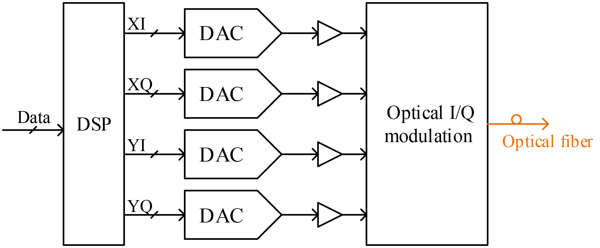
Figure 1Optical coherent transmission system (Huang et al., 2015; Cao et al., 2017; Laperle and O'Sullivan, 2014).
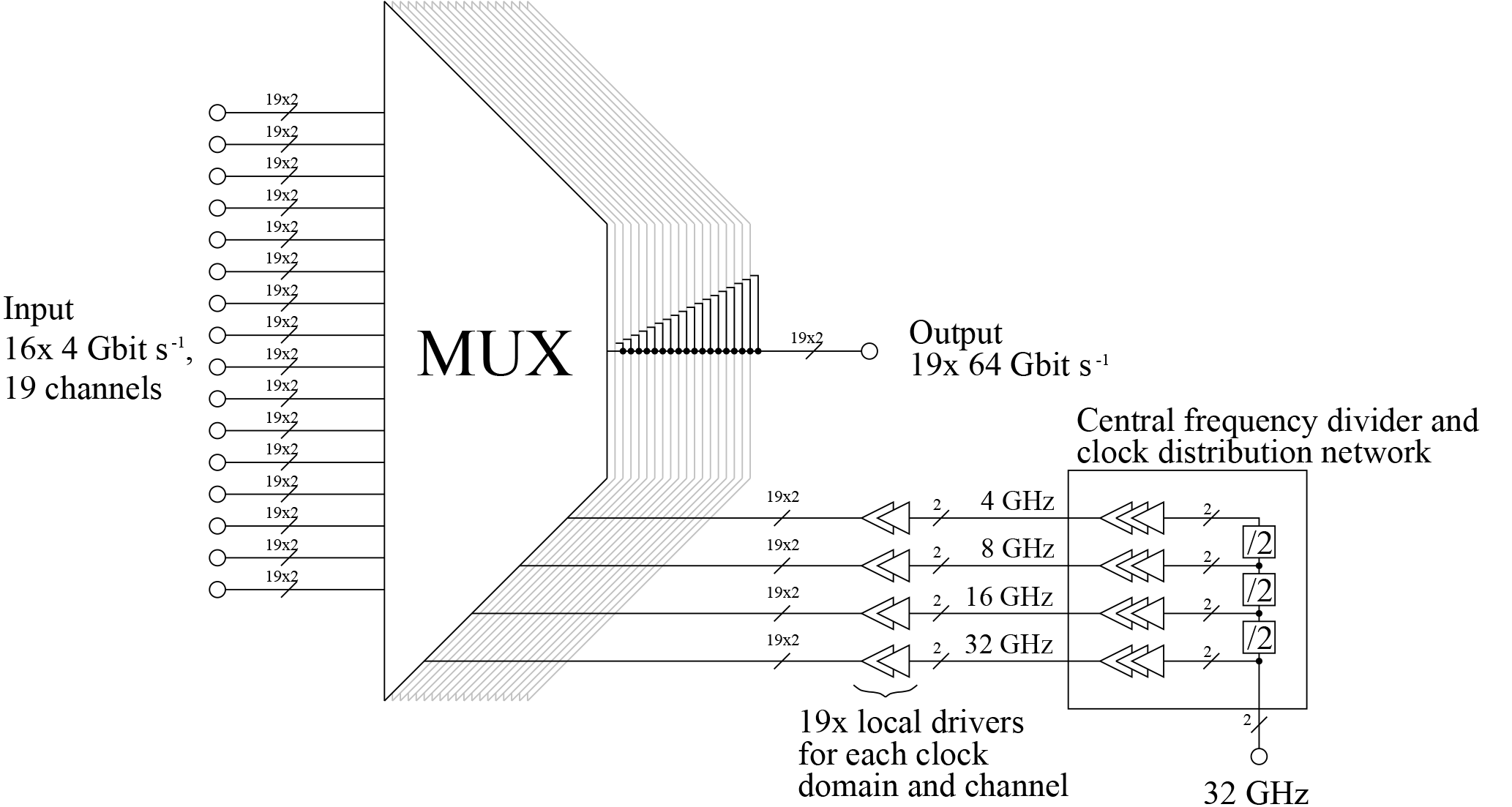
Figure 2Fully-differential serializer including the MUX and the clock network. The MUX consists of 19 identical 16:1 MUX channels, each of them provides an output data rate of 64 Gbit s−1 for an input data rate of 16 × 4 Gbit s−1. Additionally, a central frequency divider and clock distribution network generates the necessary clock signals feeding local drivers in front of all MUX channels.
The MUX is designed in the STMicroelectronics 28 nm FD-SOI CMOS technology. The technology has many advantageous features compared to deteriorating properties of transistors in conventional bulk processes. For instance, it helps reducing leakage currents, prevents latch-ups and leads to an improvement of the sub-threshold slope. Finally, FD-SOI technology allows for flip well transistors due to a buried oxide (BOX) layer of 25 nm below the thin channel of 7 nm, meaning an NMOS transistor is built on an n-well and a PMOS transistor is build on a p-well layer separated by the BOX. This specific feature enables more efficient forward body biasing within a much larger voltage range compared to bulk processes which is an advantage owing to strong threshold voltage control and faster switching processes. So, the well areas act as a back gate that can be biased independently (Magarshack et al., 2013; Noel et al., 2009, 2011; Planes et al., 2012). Figure 3 illustrates the cross section of flip well FD-SOI MOSFETs. In the system presented here, a body voltage of is applied to the n-well and a voltage of is applied to the p-well to bias the MOSFETs for low threshold voltage and high speed.
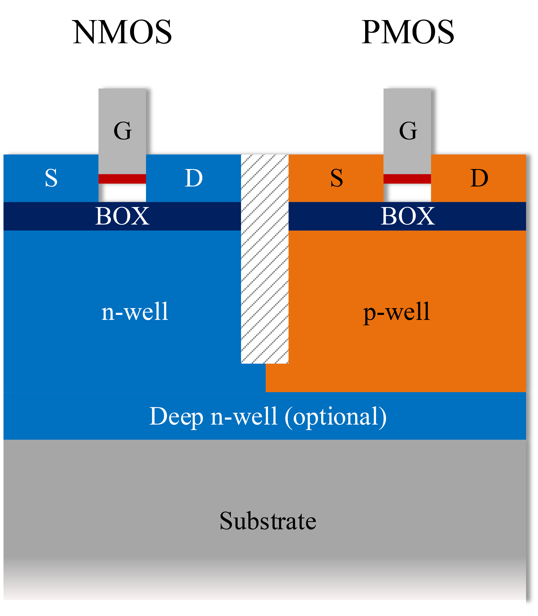
Figure 3Schematic layer structure of the used FD-SOI flip well MOSFETs according to Noel et al. (2009, 2011) (not to scale). The thin channel regions below the gates (G) are shown in white. S and D indicate the raised source and drain regions.
The fully-differential MUX consists of 19 identical 16:1 MUX channels. Figure 4a shows the block diagram of one 16:1 MUX channel. It is realized in 15 cascaded 2:1 stages, each of them consisting of five latches in a two-latch-three-latch structure and a transmission gate (TG). A detailed block diagram as well as an example for ideal input and output waveforms of a single 2:1 MUX stage are depicted in Fig. 4b and c, respectively. The configuration in Fig. 4b avoids simultaneous transitions at the TG inputs and limits the number of required differential clock phases for all clock domains to one. The need of only one differential clock phase is the main advantage of the cascaded MUX structure discussed here. Moreover, the input data is synchronous in contrast to a configuration with equal number of latches at the inputs. To generate an output data rate of 64 Gbit s−1 out of an input data rate of 4 Gbit s−1, 15 of these stages have to be cascaded in a four-stage binary tree for each of the 19 channels.
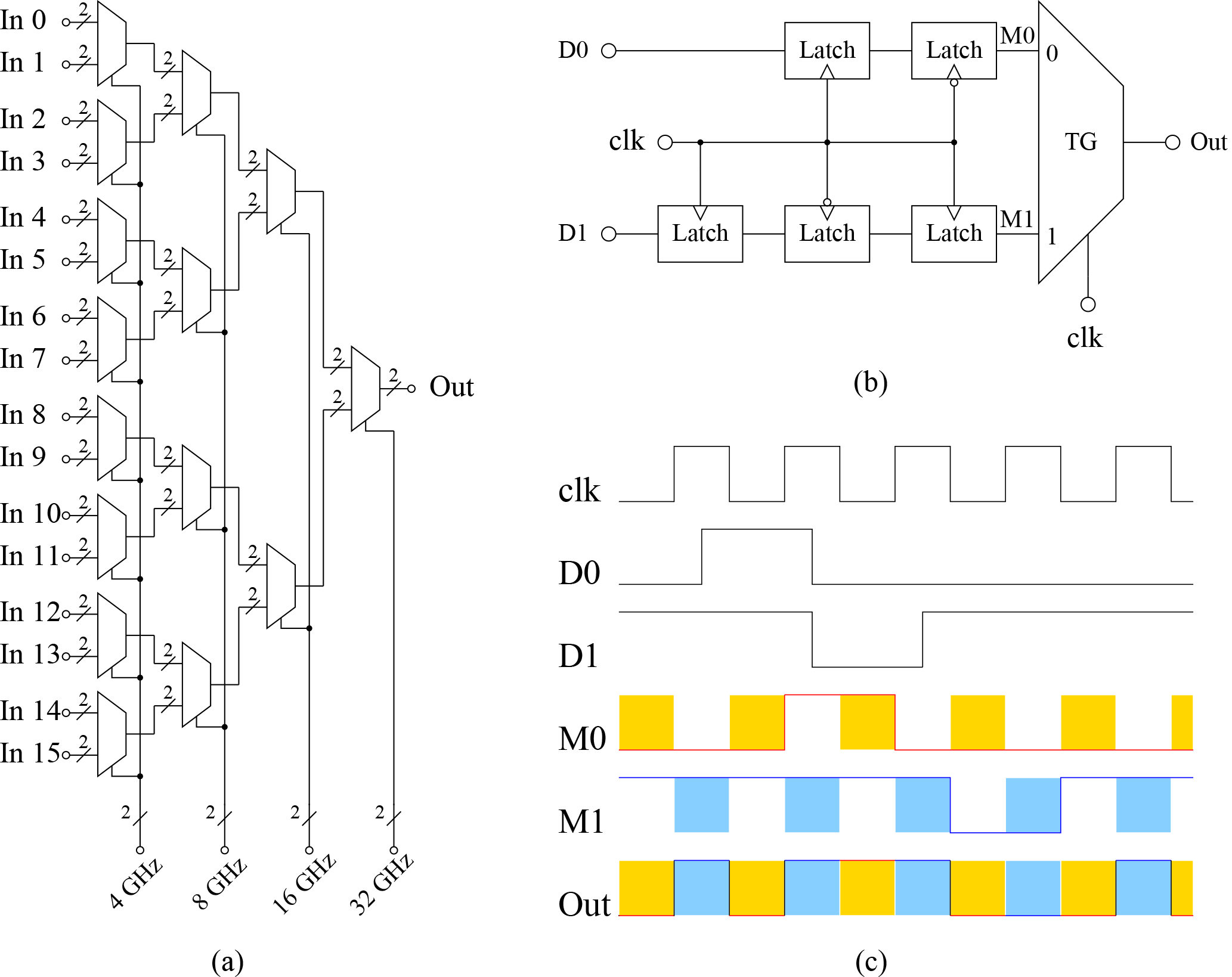
Figure 4(a) Block diagram of one 16:1 MUX channel. It consists of 15 single 2:1 MUX stages depicted as block diagram in (b). The corresponding ideal waveforms and timing for one 2:1 MUX stage are shown in single-ended form in (c). The colors indicate the transparent states of the TGs for the signals M0 (red line/yellow box) and M1 (blue line/blue box).
For clk =L, the first latches for D0 as well as D1 are transparent. The TG is transparent in the M0 path for clk =L and in the M1 path for clk =H, respectively. The realizations of the fast latches and TGs are depicted in Fig. 5. The latches consist of TGs, a clocked feedback path and output drivers.
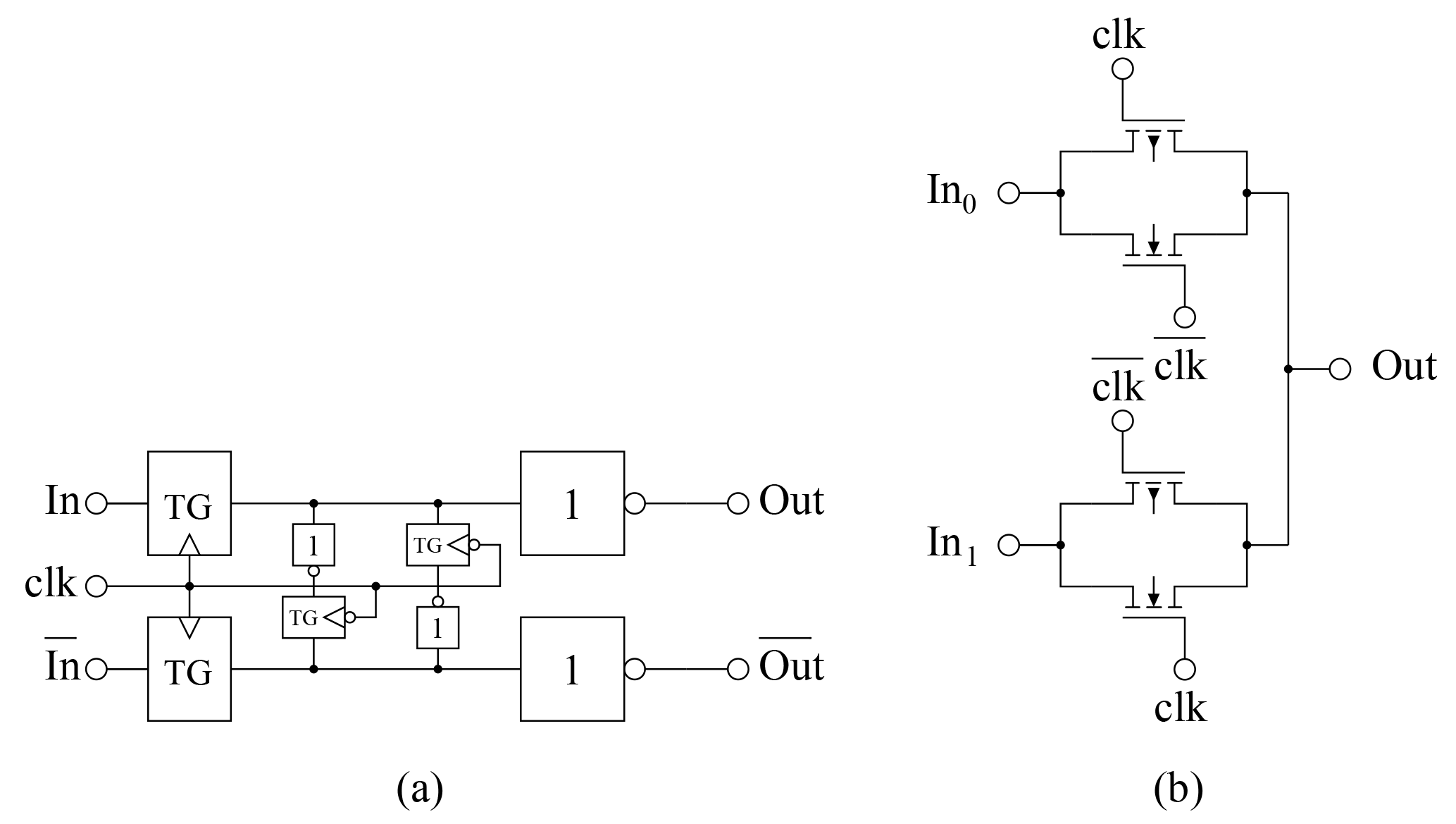
Figure 5Realization of the fast latches (a) as well as circuit of the differential TGs performing the multiplexing function (b).
To drive the whole MUX tree, four differential clocks are required with the frequencies 32, 16, 8 and 4 GHz. The input clock signal is a differential 32 GHz signal. All other clock signals are generated by flipflop-based frequency dividers. Moreover, a clock distribution tree with large drivers is necessary for operation of all 19 MUX channels. This block of clock generation and clock drivers in combination with transmission lines for distribution builds up the clock network that is shown in total in Fig. 6. As the number of latches and TGs doubles going to the next lower frequency level, the load for the clock drivers is kept the same by consequent downscaling of transistor widths in the latches and the TGs. An important issue for proper multiplexing is a precise alignment of phases, i.e. low skew of the different clock signals. This is done by a careful design of the driver chains in the different clock branches. To compensate for clock-to-output delays of the frequency dividers and different fan-outs, additional inverters of constant transistor widths (4 µm for NMOS and 8 µm for PMOS transistors) are inserted in the higher frequency branches. In the final stages, the driver capability has to be increased by a tapered cascade of inverters with an effective fan-out of approximately 1.4 to 1.5.
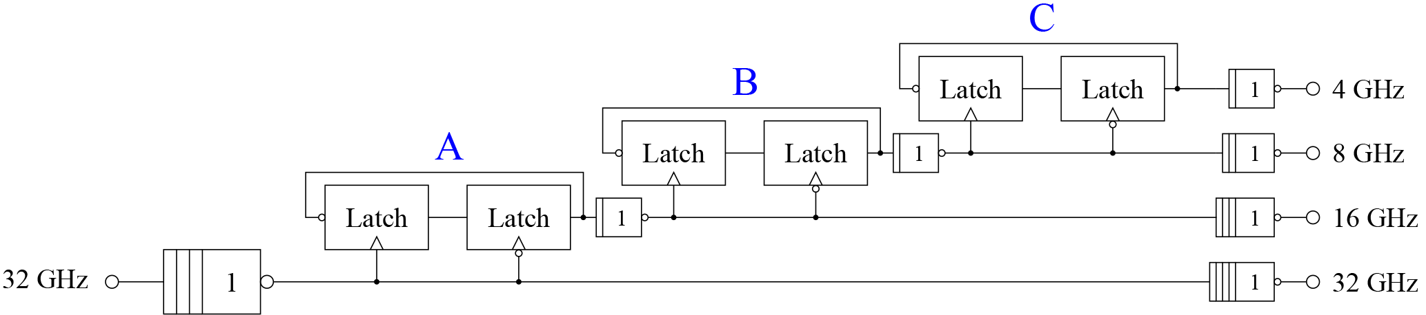
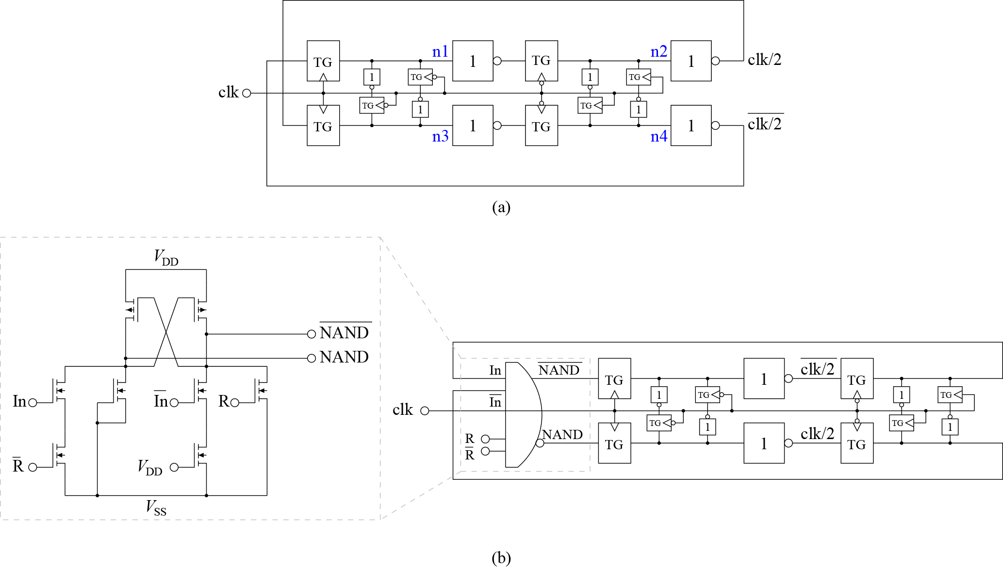
Figure 7(a) Realization of the frequency divider without reset for 32 GHz → 16 GHz and (b) frequency divider with reset for lower frequencies. Resetting is done by an additional differential NAND gate and a differential reset signal (). The frequency divider in (a) is used at position A in Fig. 6, the one in (b) is used at positions B and C.
Figure 8Clock transmission line for one clock frequency and transmission line equivalent circuit without losses for simplicity.
Figure 7 shows the realization of the different frequency dividers used in the serializer at different stages.
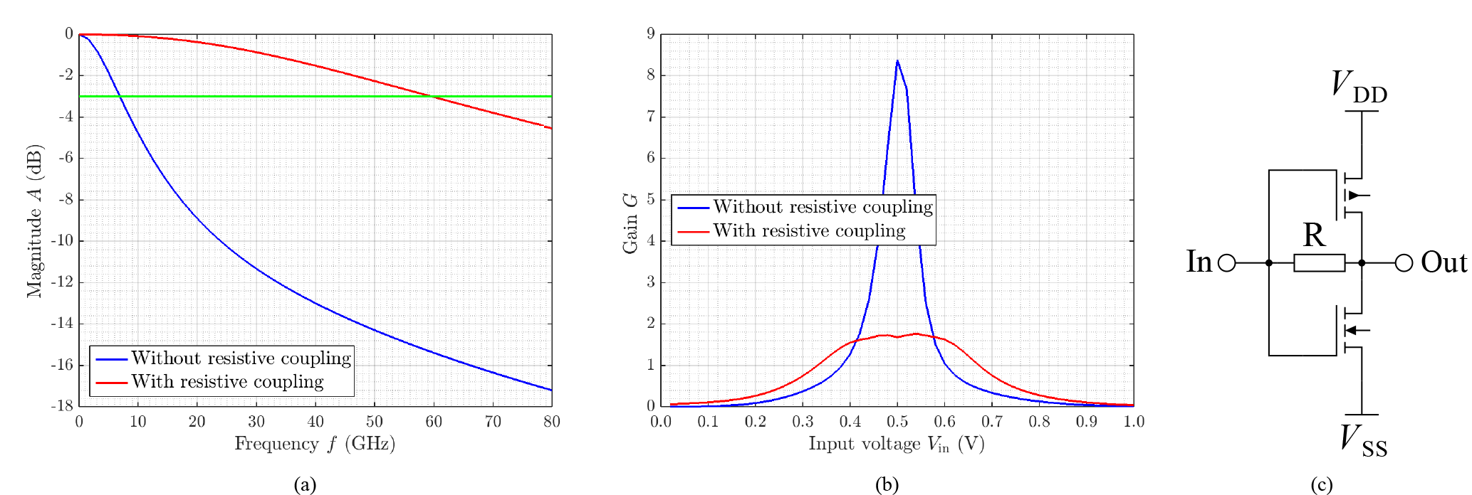
Figure 9(a) Small-signal frequency response normalized to the value at f=0 Hz and (b) small-signal gain vs. input voltage of one inverter loaded by a duplicate without and with resistive feedback on schematic level. The green line in (a) shows the −3 dB line. The DC operating point for the frequency response simulations is chosen to be 0.5 V. A resistively coupled inverter is shown on the right hand side (c).

Figure 10Eye diagrams of the signal after the 32 GHz path driver chain (single-ended) without resistive feedback (a) and with resistive feedback (b) for schematic simulations and a data rate of 64 Gbit s−1. As input source, a pseudo-random bit stream was chosen.
The frequency divider for 32 GHz (position A in Fig. 6) does not have a reset because the extra capacitive load by additional transistors would be too high for operation at 32 GHz. Therefore, the divider starts immediately with the first edge of the external clock. For initialization, minimum width pull-down NMOS transistors are inserted at the gates of the large inverters (nodes n3 and n4 in Fig. 7). For symmetry reasons, always-off NMOS transistors are placed at positions n1 and n2. In contrast to this frequency divider, the other dividers for lower frequencies (positions B and C in Fig. 6) are provided with an additional NAND gate as reset circuit (see Fig. 7b) realizing the logical function (differentially). The reset function is very important not only for initialization and starting at a dedicated time but also for a cascaded start of the whole serializer. By subsequent switching on the different frequency levels, large current jumps leading to voltage drops that can cause a collapse of the clock dividers can be omitted. The inverters in both frequency dividers have different dimensions. This ensures a comparable fan-out of the output inverters (clk∕2 and ) that are loaded externally and the other inverters.
The clock distribution through a non-terminated transmission line and the local drivers before each of the MUX channels are shown in detail in Fig. 8. The use of extra cascaded local drivers with NMOS widths Wn reaching from 4 to 12 µm (PMOS widths ) is necessary to reduce the capacitive load by a factor of 1∕3 at each transmission line tap and therefore, it increases the line impedance. Between each tap with distance 10 µm, an inductance in the order of L≈5 pH can be extracted. The capacitance is assumed to be dominated by the first local driver gate capacitance and it can be estimated to be C≈12 fF. In the transmission line equivalent circuit, the resistance is neglected in a first order approximation to show the main effect of capacitive load. Additionally, the local drivers regenerate the clock signal voltage levels (see later).

Figure 11Monte-Carlo simulation results of a long output driver chain with fan-outs of approximately 1.5 similar to the one used in the clock distribution system for 50 simulations. In (a) and (b) the results without resistive coupling, in (c) and (d) the results with resistive coupling are shown. The values of the maximum amplitude Vmax and the single-ended duty cycles with reference to 0.5 V after the long driver chain are given. In the simulations, process variations as well as mismatch are included. The mean values (μ) and the standard deviations (σ) are also given. Without feedback, a yield of only 70 % is found, i.e., in 30 % of the cases, the driver chain signal collapses with maximum below 0.5 V.
Driving a huge load of 19 16:1 MUX channels requires large clock output drivers with 80 µm NMOS width as well as 160 µm PMOS width and therefore a long tapered driver chain for each frequency domain. In the case of the 32 GHz frequency domain, the bandwidth of the 22 stage CMOS inverters chain is right at the edge of proper operation. The long chain is required for delay compensation and reaching the required output driver capability. Considering layout effects and process variations makes a further increase of their bandwidth necessary. In order to omit a massive shift of the average voltage away from 0.5 V preventing the 32 GHz clock signal from passing through the driver chain, a resistive feedback (see Fig. 9c) similar to analog amplifiers is introduced in the inverters, like e.g. in Wu et al. (2005) and Chao et al. (2008). The frequency response normalized to the value at f=0 Hz and the small-signal gain function of one inverter with and without feedback loaded by a duplicate are shown in Fig. 9. It becomes obvious that the small-signal −3 dB bandwidth increases from about 7 to about 60 GHz by introducing resistive feedback and the inverter is linearized because the gain is constant over a larger input voltage range. However, it is much smaller. The coupling prevents the long inverter chain from not being functional leading to constant outputs as a change in the average input voltage away from 0.5 V is not that critical like in the non-coupled case. Owing to that, this concept is also interesting for data paths. The output signals of the inverter chain of the 32 GHz path with 22 inverters without as well as with resistive feedback are compared in Fig. 10 on schematic level. For the visualization of bandwidth and data-dependent jitter considerations, the inverter chain is excited by a pseudo-random bit stream instead of a clock signal. Obviously, the data-dependent jitter can be decreased from approximately 5 to about 1 ps with resistive feedback due to linearization and small-signal bandwidth increase although the large-signal rise and fall times are not improved. The increase in bandwidth is at the expense of a lower gain, more power consumption and voltage level degeneration that can be directly seen in the eye diagrams in Fig. 10. To compensate for level degeneration, the local drivers not being resistively coupled regenerate the voltage levels of the clock signals to a certain extend in addition to the already mentioned decrease of the capacitive load. Moreover, the clock dividers are loaded by inverters without coupling, too.
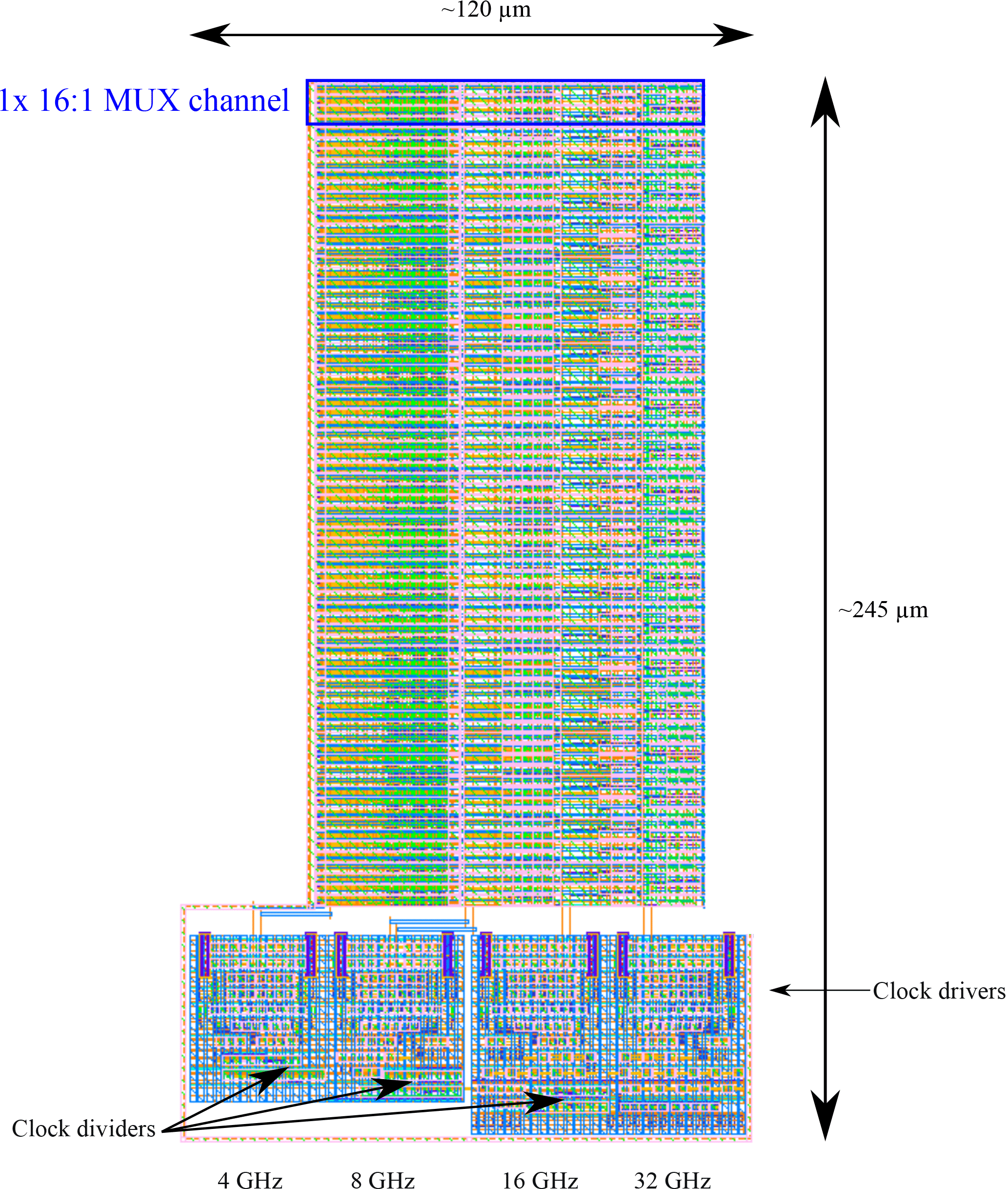
Figure 12Layout of the whole serializer. In the lower part, the frequency dividers and clock drivers can be identified for all four clock domains whereas in the upper part, the 16:1 MUX channels are located. The size of a single MUX channel is indicated by a blue box.
As there is a trade-off between an increasing bandwidth on the one hand and power consumption, voltage level degeneration as well as gain reduction on the other hand, we chose the design rule for the feedback resistance R as a function of the NMOS transistor width Wn according to Eq. (1). The PMOS transistor width Wp is always twice Wn. That way, a maximum small-signal gain between 1.5 and 2 is still reached (see Fig. 9b).
Another essential requirement for the clock network is the reliability over process variations. Therefore, Monte-Carlo simulations including process variations and mismatch have been carried out to identify the system's variability. Owing to a huge netlist of the clock network extraction, these statistical simulations are performed on a schematic level. However, to estimate layout effects, the simulated frequency is chosen to be approximately 35 % larger, i.e. 43 GHz, which is a worst-case value essentially based on the expected slowdown of design due to layout capacitance. A slowdown of 35 % is assumed to be a worst case value based on extraction results of a delay cell with slow transistor corners. The simulation results in Fig. 11 illustrate the advantage of resistively coupled inverter chains. First, the maximum values of the clock output signals are considered. On the one hand, the yield for the non-coupled chain is only 70 % which can be seen in the top left figure. For some cases, the maximum output voltage is less than 0.5 V which essentially means a collapse of the signal. On the other hand, the maximum voltage values of the coupled chain are always well beyond 0.5 V indicating a proper operation. Nevertheless, the voltage degeneration can be observed clearly. These simulations were carried out for an output driver stage of only 13 inverters. For the whole 32 GHz path, the non-coupled inverter chain does not work anymore at the given frequency. Secondly, the (single-ended) duty cycles with reference to 0.5 V are of particular importance for proper operation (see right figures in Fig. 11). Whereas the duty cycles in the non-coupled case are mostly below the seeked value of 50 %, the duty cycles in the case of coupled inverters are closer to 50 % for the most part.
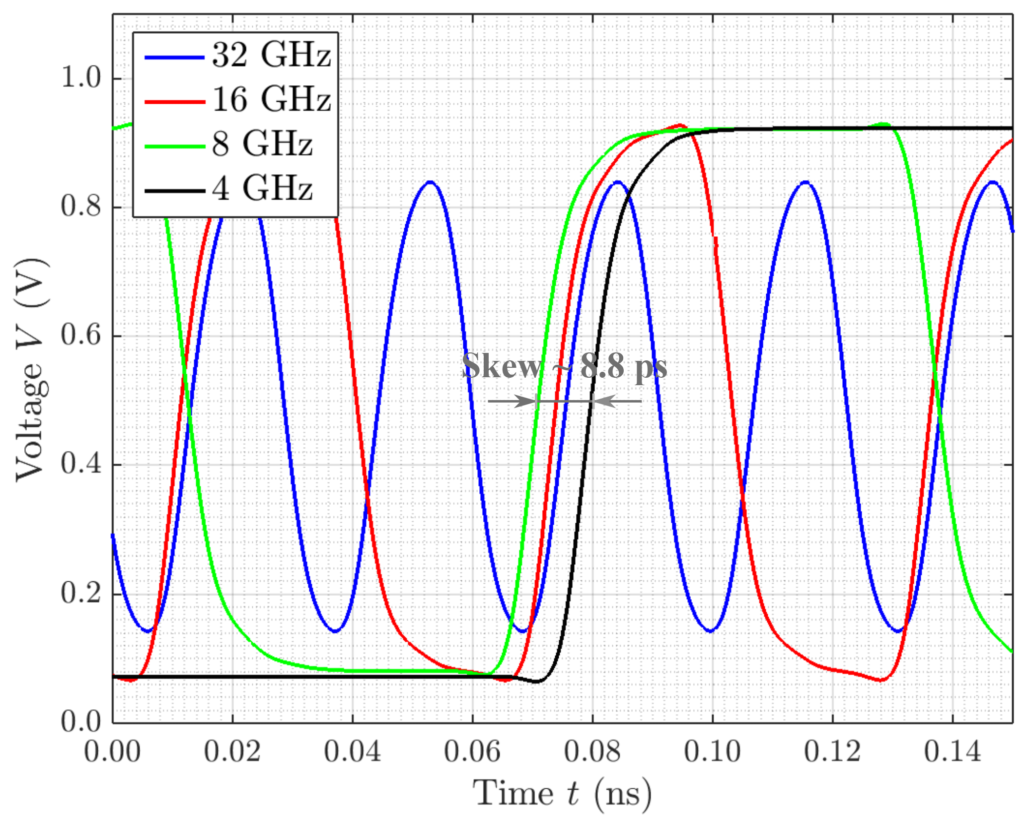
Figure 13Single-ended output of the clock network for resistive and capacitive parasitics extraction. The skew of all four clock signals is indicated.
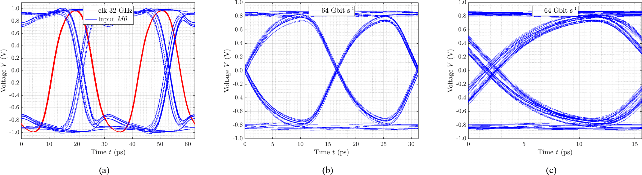
Figure 14Eye diagrams at the input (a) and output (b, c) of the last 2:1 MUX stage with an output data rate of 64 Gbit s−1 for 200 transitions. Plot (b) shows the eyes of the two input channels separately, plot (c) shows them in one eye diagram for a period of 15.625 ps.
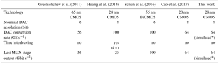
Table 1Comparison of the last serializer stages in state-of-the-art high speed DACs.
* Extraction including resistive and capacitive parasitics and additionally inductances for the clock transmission lines.
To summarize, the static CMOS operating frequency can be increased by resistive feedback leading to reliable functionality of the clock network. In contrast to current mode logic (CML) circuits, no extra supply voltages are required which is an advantage. This concept is completely compatible with static CMOS logic circuits and their power supply. However, the disadvantages of resistively coupled inverter chains are a reduced gain (gain-bandwidth product), degenerated voltage levels (see Fig. 9b) and a much higher average power consumption. One positive effect of the higher static power consumption is the relaxation of current peaks during the switching on process. However, it is a big drawback for the envisaged low power CMOS system.
In Fig. 12, the complete serializer layout with the dimensions of approximately 245 µm × 120 µm is depicted. At the bottom, the frequency dividers as well as the clock trees for the different frequency domains can be seen. On the upper part, the 19 vertically shifted 16:1 MUX channels are visible.
The following simulations include resistive and capacitive parasitics extraction. Additionally, the clock transmission lines are extracted considering also inductance. For simplicity, only one MUX channel is shown here. For the clock network, a skew of about 8.8 ps for the different frequencies can be extracted from Fig. 13 which fulfills one condition for proper operation of the MUX at all input clock frequencies up to 32 GHz. Other important conditions are a low data path skew, temperature stability as well as parameter mismatch and variations tolerance. As the clock signals are propagating through transmission lines, the delay in the different MUX stages due to this propagation requires the DAC output to be at the top in Fig. 12. That way, the clock signal and the analog output signal propagate in the same direction and the delays proceed similarly in the clock transmission line or in the analog line, respectively.
In Fig. 14, the timing at the last 2:1 MUX stage for 64 Gbit s−1 for one input is shown on the left hand side. The TG is transparent for clk =L and it becomes obvious that a skew of several picoseconds between the 32 and the 16 GHz clock signals can be tolerated. A margin of approximately +5 and −10 ps is estimated from Fig. 14a for the 32 GHz clock signal referred to the 16 GHz clock signal. Lower frequency stages have a margin of a multiple. The eye diagrams at the output of the last 2:1 MUX stage are presented in Fig. 14b and c for both input channels separately (b) and in total (c). They reveal a data-dependent peak-to-peak jitter of less than 830 fs for the single eyes of both input channels. Owing to a still non-perfect duty cycle of the 32 GHz clock signal which is already indicated in Fig. 11d, the horizontal eye openings for the two depicted channels are not completely symmetrical. A difference of approximately 2 ps can be stated in the horizontal eye opening depending on process parameters. Considering also the effect of non-perfect clock duty cycle, the data-dependent jitter increases to approximately 1.73 ps (Fig. 14c). To improve the duty cycle of the 32 GHz clock signal, an already increased positive supply voltage of 1.1 V is applied to the clock output drivers. However, MUX, clock dividers and local clock drivers are operated at standard 1.0 V supply voltage. Generally, to compensate for the different eye openings, one can e.g. further vary the supply voltage of the driver network or add an appropriate pre-distortion to the 32 GHz input clock signal.
The total average power consumption of the system Ptotal consisting of the MUX and local drivers part PMUX+loc. drivers as well as the clock network part Pclock network is given in Eq. (2).
The power consumption is dominated by the clock network. Its contribution is Pclock network≈600 mW and a major part of the local drivers contributes to PMUX+loc. drivers≈550 mW. Due to the proximity of the local drivers and the MUX stages, the MUX has to share its power supply with the local drivers. Finally, the power consumption requires an adequate cooling concept which is realized by thinned chips (≤ 150 µm) and active cooling.
To conclude, a serializer with a 19 channel 16:1 MUX including a frequency divider and clock distribution network for output data rates up to 64 Gbit s−1 is shown. Simulations with parasitic extraction reveal a data-dependent peak-to-peak jitter of less than 1.8 ps at the output of one MUX channel, a total average power consumption of approximately 1.15 W of the whole serializer and potentially 1.216 Tbit s−1 throughput. This circuit can be used together with an output stage and a resistance network in an 8 bit 64 GS s−1 DAC with four bits unary and four bits binary segmentation for optical communication systems or AWGs. Table 1 shows the DACs with highest conversion rates and the output data rate of their last digital front-end serializer stages. The DAC front-end MUX stage presented here reveals one of the highest output data rates in CMOS technology to the best of the authors' knowledge. Only in bipolar technology, significant faster multiplexing is achieved (Schuh et al., 2016). Simulation results are comparable to the serializer in Cao et al. (2017) but the speed is achieved in the 28 nm technology node and in static CMOS logic (modified by resistive coupling) instead of CML. The main advantages of this circuit are the high output data rates up to 64 Gbit s−1, the static CMOS compatibility concerning supply voltages and the requirement of only one differential clock phase for all frequency domains. For high-speed DAC applications, the shown results are very promising.
The simulation data that support the findings of this study are available in Zenodo with the identifier https://doi.org/10.5281/zenodo.1283303 (Widmann et al., 2018).
The authors declare that they have no conflict of interest.
This article is part of the special issue “Kleinheubacher Berichte 2017”. It is a result of the Kleinheubacher Tagung 2017, Miltenberg, Germany, 25–27 September 2017.
This research is supported by Deutsche Forschungsgemeinschaft (DFG – BE
2256/27-1).
Edited by: Dirk
Killat
Reviewed by: two anonymous referees
Cao, J., Cui, D., Nazemi, A., He, T., Li, G., Catli, B., Khanpour, M., Hu, K., Ali, T., Zhang, H., Yu, H., Rhew, B., Sheng, S., Shim, Y., Zhang, B., and Momtaz, A.: A transmitter and receiver for 100Gb/s coherent networks with integrated 4x64GS/s 8b ADCs and DACs in 20nm CMOS, in: 2017 IEEE International Solid-State Circuits Conference (ISSCC), 484–485, 2017. a, b, c, d
Chao, S. F., Kuo, J. J., Lin, C. L., Tsai, M. D., and Wang, H.: A DC-11.5 GHz Low-Power, Wideband Amplifier Using Splitting-Load Inductive Peaking Technique, IEEE Microw. Wirel. Co., 18, 482–484, 2008. a
Greshishchev, Y. M., Pollex, D., Wang, S. C., Besson, M., Flemeke, P., Szilagyi, S., Aguirre, J., Falt, C., Ben-Hamida, N., Gibbins, R., and Schvan, P.: A 56GS/S 6b DAC in 65nm CMOS with 256x6b memory, in: 2011 IEEE International Solid-State Circuits Conference, 194–196, 2011. a
Huang, H., Heilmeyer, J., Grözing, M., and Berroth, M.: An 8-bit 100-GS/s distributed DAC in 28-nm CMOS, IEEE Rad. Freq. Integr., 65–68, 2014. a
Huang, H., Heilmeyer, J., Grözing, M., Berroth, M., Leibrich, J., and Rosenkranz, W.: An 8-bit 100-GS/s Distributed DAC in 28-nm CMOS for Optical Communications, IEEE T. Microw. Theory, 63, 1211–1218, 2015. a, b
Laperle, C. and O'Sullivan, M.: Advances in High-Speed DACs, ADCs, and DSP for Optical Coherent Transceivers, J. Lightwave Technol., 32, 629–643, 2014. a, b
Magarshack, P., Flatresse, P., and Cesana, G.: UTBB FD-SOI: A Process/Design Symbiosis for Breakthrough Energy-efficiency, in: Proceedings of the Conference on Design, Automation and Test in Europe, 952–957, 2013. a
Noel, J. P., Thomas, O., Fenouillet-Beranger, C., Jaud, M. A., Scheiblin, P., and Amara, A.: A simple and efficient concept for setting up multi-VT devices in thin BOx fully-depleted SOI technology, in: 2009 Proceedings of the European Solid State Device Research Conference, 137–140, 2009. a, b
Noel, J. P., Thomas, O., Jaud, M. A., Weber, O., Poiroux, T., Fenouillet-Beranger, C., Rivallin, P., Scheiblin, P., Andrieu, F., Vinet, M., Rozeau, O., Boeuf, F., Faynot, O., and Amara, A.: Multi-VT UTBB FDSOI Device Architectures for Low-Power CMOS Circuit, IEEE T. Electron Dev., 58, 2473–2482, 2011. a, b
Planes, N., Weber, O., Barral, V., Haendler, S., Noblet, D., Croain, D., Bocat, M., Sassoulas, P. O., Federspiel, X., Cros, A., Bajolet, A., Richard, E., Dumont, B., Perreau, P., Petit, D., Golanski, D., Fenouillet-Béranger, C., Guillot, N., Rafik, M., Huard, V., Puget, S., Montagner, X., Jaud, M. A., Rozeau, O., Saxod, O., Wacquant, F., Monsieur, F., Barge, D., Pinzelli, L., Mellier, M., Boeuf, F., Arnaud, F., and Haond, M.: 28nm FDSOI technology platform for high-speed low-voltage digital applications, in: 2012 Symposium on VLSI Technology (VLSIT), 133–134, 2012. a
Schuh, K., Buchali, F., Idler, W., Hu, Q., Templ, W., Bielik, A., Altenhain, L., Langenhagen, H., Rupeter, J., Duemler, U., Ellermeyer, T., Schmid, R., and Moeller, M.: 100 GSa/s BiCMOS DAC Supporting 400 Gb/s Dual Channel Transmission, in: ECOC 2016, 42nd European Conference on Optical Communication, 1–3, 2016. a, b
Widmann, D., Grözing, M., and Berroth, M.: High-Speed Serializer for a 64 GS/s Digital-to-Analog Converter in a 28 nm Fully-Depleted Silicon-on-Insulator CMOS Technology [Data set], Zenodo, https://doi.org/10.5281/zenodo.1283303, 2018. a
Wu, C.-H., Lee, C.-H., Chen, W.-S., and Liu, S.-I.: CMOS wideband amplifiers using multiple inductive-series peaking technique, IEEE J. Solid-St. Circ., 40, 548–552, 2005. a